

Zie specificaties voor productdetails.
XC7K410T-2FFG900C
Product Overview
Category
The XC7K410T-2FFG900C belongs to the category of Field-Programmable Gate Arrays (FPGAs).
Use
FPGAs are integrated circuits that can be programmed after manufacturing, allowing for flexible and customizable digital circuit designs. The XC7K410T-2FFG900C is specifically designed for high-performance applications.
Characteristics
- High-performance FPGA with advanced features
- Programmable logic cells for custom circuit implementation
- Integrated memory blocks for data storage
- High-speed serial transceivers for fast data communication
- Flexible I/O interfaces for connecting with external devices
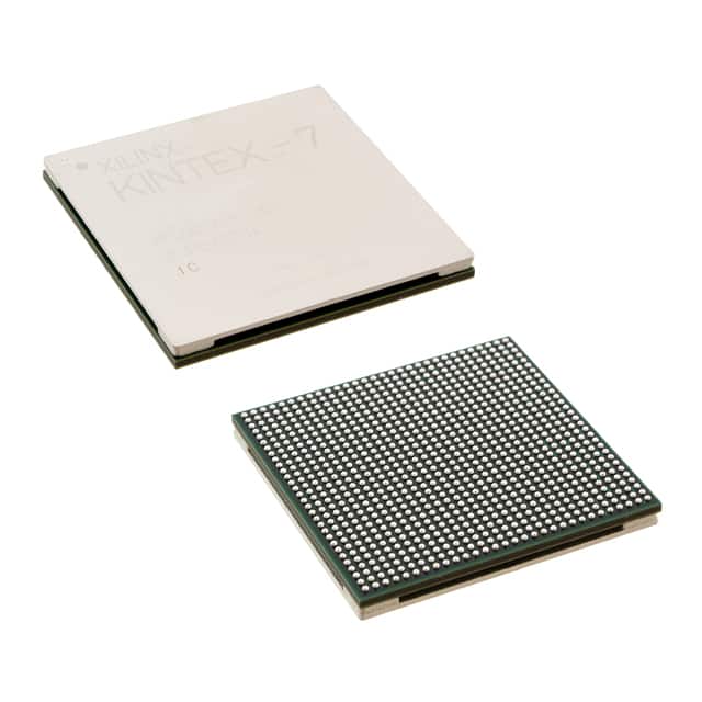
Package
The XC7K410T-2FFG900C comes in a compact package suitable for surface-mount technology (SMT) assembly. It is designed to be mounted on printed circuit boards (PCBs) for integration into electronic systems.
Essence
The essence of the XC7K410T-2FFG900C lies in its ability to provide a highly configurable and reprogrammable hardware platform for implementing complex digital circuits.
Packaging/Quantity
The XC7K410T-2FFG900C is typically packaged in trays or reels, depending on the manufacturer's specifications. The quantity per package may vary, but it is commonly available in quantities suitable for both prototyping and production purposes.
Specifications
- FPGA Family: Kintex-7
- Device: XC7K410T
- Logic Cells: 410,000
- Memory Blocks: 1,800
- DSP Slices: 1,920
- Maximum I/O Pins: 500
- Transceivers: 16
- Operating Voltage: 1.2V
- Package Type: FFG900C
Detailed Pin Configuration
The XC7K410T-2FFG900C has a comprehensive pin configuration, allowing for versatile connectivity options. The detailed pinout information can be found in the product datasheet provided by the manufacturer.
Functional Features
1. High Performance
The XC7K410T-2FFG900C offers high-performance capabilities, making it suitable for demanding applications that require fast processing and data throughput.
2. Configurability
With its programmable logic cells, the XC7K410T-2FFG900C allows users to implement custom digital circuits tailored to their specific requirements. This flexibility enables rapid prototyping and design iterations.
3. Integrated Memory
The integrated memory blocks provide on-chip storage for data processing, reducing the need for external memory components and improving overall system performance.
4. High-Speed Serial Transceivers
The XC7K410T-2FFG900C features high-speed serial transceivers, enabling fast communication with other devices or systems using protocols such as PCIe, SATA, or Ethernet.
5. Flexible I/O Interfaces
The FPGA offers a wide range of I/O interfaces, including LVCMOS, LVDS, and differential signaling, allowing for seamless integration with various external devices and peripherals.
Advantages and Disadvantages
Advantages
- High configurability and flexibility
- High-performance capabilities
- Integrated memory blocks for efficient data processing
- Support for high-speed serial communication
- Versatile I/O interface options
Disadvantages
- Steeper learning curve compared to traditional fixed-function integrated circuits
- Higher power consumption compared to dedicated application-specific integrated circuits (ASICs)
- Relatively higher cost per unit compared to mass-produced standard integrated circuits
Working Principles
The XC7K410T-2FFG900C operates based on the principles of reconfigurable computing. It consists of an array of programmable logic cells interconnected through configurable routing resources. The user designs a digital circuit using a hardware description language (HDL) and programs it onto the FPGA. During operation, the FPGA executes the programmed circuit by configuring its internal resources accordingly.
Detailed Application Field Plans
The XC7K410T-2FFG900C finds applications in various fields that require high-performance digital circuit implementation. Some potential application areas include:
- Telecommunications: Implementing signal processing algorithms for wireless communication systems.
- Aerospace and Defense: Designing radar and sonar signal processing systems.
- High-Performance Computing: Accelerating computationally intensive tasks such as scientific simulations or data analytics.
- Industrial Automation: Developing custom control systems for manufacturing processes.
- Medical Imaging: Implementing real-time image processing algorithms for medical imaging devices.
Detailed and Complete Alternative Models
- XC7K325T-2FFG900C: A lower-capacity variant of the same FPGA family, suitable for applications with less demanding requirements.
- XC7K480T-2FFG900C: A higher-capacity variant of
Noem 10 veelgestelde vragen en antwoorden met betrekking tot de toepassing van XC7K410T-2FFG900C in technische oplossingen
Sure! Here are 10 common questions and answers related to the application of XC7K410T-2FFG900C in technical solutions:
Question: What is XC7K410T-2FFG900C?
- Answer: XC7K410T-2FFG900C is a specific model of Xilinx's Kintex-7 FPGA family, which offers high-performance programmable logic for various technical applications.Question: What are the key features of XC7K410T-2FFG900C?
- Answer: Some key features of XC7K410T-2FFG900C include a large number of programmable logic cells, high-speed serial transceivers, integrated memory blocks, and advanced DSP capabilities.Question: What are the typical applications of XC7K410T-2FFG900C?
- Answer: XC7K410T-2FFG900C is commonly used in applications such as wireless communication systems, video processing, industrial automation, aerospace, and defense.Question: How can XC7K410T-2FFG900C be programmed?
- Answer: XC7K410T-2FFG900C can be programmed using Xilinx's Vivado Design Suite, which provides a comprehensive development environment for FPGA designs.Question: What is the power consumption of XC7K410T-2FFG900C?
- Answer: The power consumption of XC7K410T-2FFG900C depends on the specific design and operating conditions. It is recommended to refer to the datasheet for detailed power specifications.Question: Can XC7K410T-2FFG900C interface with other components or devices?
- Answer: Yes, XC7K410T-2FFG900C supports various standard interfaces such as PCIe, Ethernet, USB, and DDR3 memory, allowing it to easily interface with other components or devices.Question: What is the maximum operating frequency of XC7K410T-2FFG900C?
- Answer: The maximum operating frequency of XC7K410T-2FFG900C depends on the specific design and implementation constraints. It is recommended to perform timing analysis during the design process.Question: Can XC7K410T-2FFG900C be used in safety-critical applications?
- Answer: Yes, XC7K410T-2FFG900C can be used in safety-critical applications. However, it is important to follow appropriate design practices and consider necessary safety measures.Question: Are there any development boards available for XC7K410T-2FFG900C?
- Answer: Yes, Xilinx offers development boards specifically designed for XC7K410T-2FFG900C, which provide a convenient platform for prototyping and testing.Question: Where can I find more information about XC7K410T-2FFG900C?
- Answer: You can find more detailed information about XC7K410T-2FFG900C, including datasheets, user guides, and application notes, on Xilinx's official website or by contacting their technical support.