

Zie specificaties voor productdetails.
XC7A200T-L1SBG484I
Product Overview
Category
The XC7A200T-L1SBG484I belongs to the category of Field-Programmable Gate Arrays (FPGAs).
Use
FPGAs are integrated circuits that can be programmed and reprogrammed to perform various digital functions. The XC7A200T-L1SBG484I is specifically designed for high-performance applications that require complex logic functions.
Characteristics
- High-performance FPGA with advanced features
- Large capacity and high-speed processing capabilities
- Flexible and reconfigurable design
- Low power consumption
- Suitable for a wide range of applications
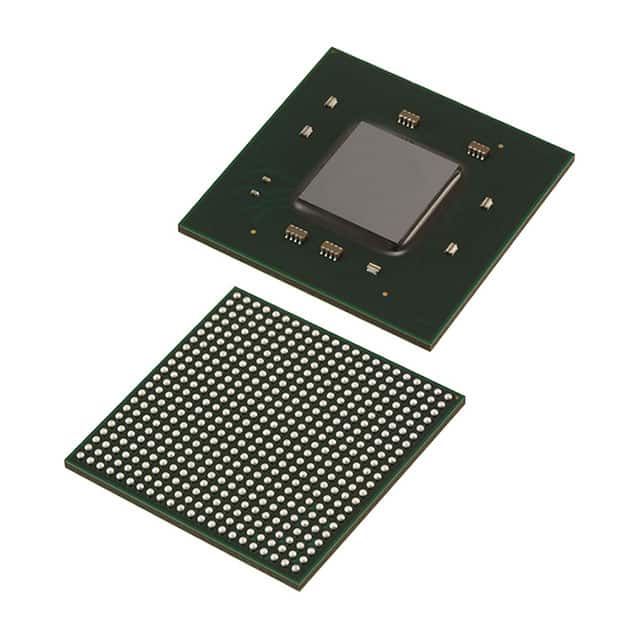
Package
The XC7A200T-L1SBG484I comes in a Ball Grid Array (BGA) package, which provides a compact and reliable form factor for easy integration into electronic systems.
Essence
The essence of the XC7A200T-L1SBG484I lies in its ability to provide a customizable hardware platform that can be tailored to specific application requirements. It offers a high level of flexibility and performance, making it suitable for demanding applications.
Packaging/Quantity
The XC7A200T-L1SBG484I is typically sold in trays or reels, depending on the manufacturer's packaging standards. The quantity per package may vary, but it is commonly available in quantities suitable for both prototyping and production purposes.
Specifications
- FPGA Family: Xilinx 7 Series
- Device Type: Artix-7
- Logic Cells: 215,360
- CLB Flip-Flops: 430,720
- Block RAM: 4,860 Kb
- DSP Slices: 740
- Maximum Frequency: 800 MHz
- Operating Voltage: 1.2V
- I/O Voltage: 3.3V
- Package Type: BGA
- Package Pins: 484
Detailed Pin Configuration
The XC7A200T-L1SBG484I has a total of 484 pins, each serving a specific purpose in the FPGA's functionality. The pin configuration includes input/output (I/O) pins, power supply pins, clock pins, and configuration pins. A detailed pinout diagram can be found in the product datasheet.
Functional Features
1. High Performance
The XC7A200T-L1SBG484I offers high-speed processing capabilities, allowing for efficient execution of complex logic functions. It is designed to handle demanding applications that require real-time processing and low-latency responses.
2. Reconfigurability
One of the key advantages of FPGAs is their ability to be reprogrammed on-the-fly. The XC7A200T-L1SBG484I allows users to modify the hardware configuration to adapt to changing requirements without the need for costly hardware redesigns.
3. Low Power Consumption
Despite its high-performance capabilities, the XC7A200T-L1SBG484I is designed to minimize power consumption. This makes it suitable for battery-powered devices or applications where energy efficiency is crucial.
4. Versatility
The XC7A200T-L1SBG484I supports a wide range of interfaces and protocols, making it compatible with various communication standards. This versatility enables seamless integration into diverse application domains.
Advantages and Disadvantages
Advantages
- High-performance processing capabilities
- Reconfigurable design for flexibility
- Low power consumption
- Versatile compatibility with different interfaces
- Large capacity for complex applications
Disadvantages
- Steeper learning curve compared to traditional microcontrollers
- Higher cost compared to off-the-shelf microcontrollers for simple applications
- Requires specialized tools and expertise for development and programming
Working Principles
The XC7A200T-L1SBG484I operates based on the principles of digital logic. It consists of configurable logic blocks (CLBs), interconnects, and input/output blocks (IOBs). The CLBs contain look-up tables (LUTs) that can be programmed to implement desired logic functions. The interconnects provide routing paths between different components, allowing for data flow and communication. The IOBs handle the interface between the FPGA and external devices.
Detailed Application Field Plans
The XC7A200T-L1SBG484I finds applications in various fields, including:
- Telecommunications: Used in high-speed data processing, signal modulation/demodulation, and protocol conversion.
- Industrial Automation: Enables real-time control systems, motor control, and sensor interfacing.
- Aerospace and Defense: Utilized in radar systems, avionics, and secure communications.
- Medical Devices: Supports image processing, patient monitoring, and diagnostic equipment.
- Automotive: Used in advanced driver-assistance systems (ADAS), infotainment systems, and engine control units.
#
Noem 10 veelgestelde vragen en antwoorden met betrekking tot de toepassing van XC7A200T-L1SBG484I in technische oplossingen
Sure! Here are 10 common questions and answers related to the application of XC7A200T-L1SBG484I in technical solutions:
Q1: What is XC7A200T-L1SBG484I? A1: XC7A200T-L1SBG484I is a specific model of Xilinx Artix-7 FPGA (Field-Programmable Gate Array) that offers high-performance processing capabilities for various technical applications.
Q2: What are the key features of XC7A200T-L1SBG484I? A2: Some key features of XC7A200T-L1SBG484I include a large number of programmable logic cells, high-speed I/O interfaces, embedded memory blocks, DSP slices, and support for various communication protocols.
Q3: What are the typical applications of XC7A200T-L1SBG484I? A3: XC7A200T-L1SBG484I is commonly used in applications such as industrial automation, aerospace systems, telecommunications, medical devices, image and video processing, and high-performance computing.
Q4: How can XC7A200T-L1SBG484I be programmed? A4: XC7A200T-L1SBG484I can be programmed using hardware description languages (HDLs) like VHDL or Verilog, which allow designers to describe the desired functionality of the FPGA.
Q5: Can XC7A200T-L1SBG484I be reprogrammed after deployment? A5: Yes, XC7A200T-L1SBG484I is a reprogrammable FPGA, meaning its configuration can be changed even after it has been deployed in a system.
Q6: What tools are available for designing with XC7A200T-L1SBG484I? A6: Xilinx provides a suite of design tools, such as Vivado Design Suite, which includes synthesis, simulation, and implementation tools specifically tailored for designing with XC7A200T-L1SBG484I.
Q7: What is the power consumption of XC7A200T-L1SBG484I? A7: The power consumption of XC7A200T-L1SBG484I depends on various factors, including the design complexity, clock frequency, and utilization of different resources. It is important to refer to the datasheet and power estimation tools provided by Xilinx for accurate power analysis.
Q8: Can XC7A200T-L1SBG484I interface with other components or devices? A8: Yes, XC7A200T-L1SBG484I supports various communication protocols like PCIe, Ethernet, USB, SPI, I2C, and UART, allowing it to interface with a wide range of components and devices.
Q9: Are there any development boards available for XC7A200T-L1SBG484I? A9: Yes, Xilinx offers development boards like the Arty A7-200T, which are specifically designed to facilitate prototyping and development with XC7A200T-L1SBG484I.
Q10: Where can I find more information about XC7A200T-L1SBG484I? A10: You can find more detailed information about XC7A200T-L1SBG484I, including datasheets, user guides, and application notes, on the official Xilinx website or by contacting Xilinx support.