

Zie specificaties voor productdetails.
XC6VHX250T-2FF1154I
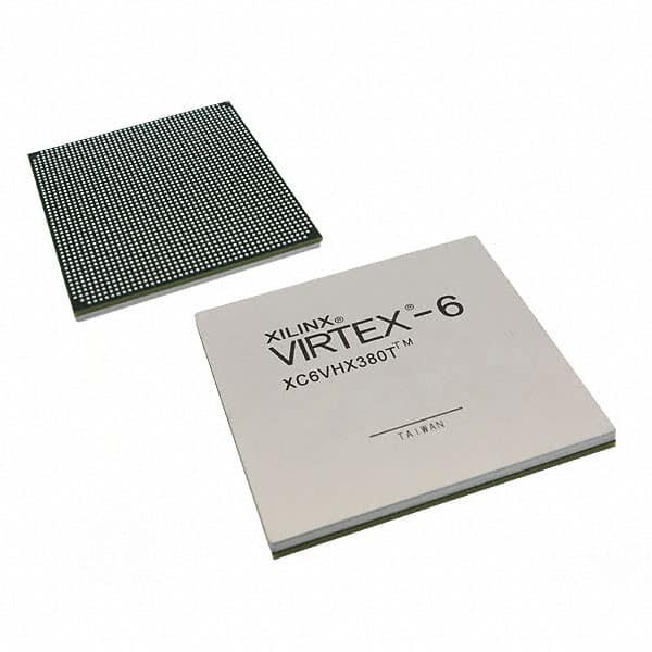
Product Overview
Category
The XC6VHX250T-2FF1154I belongs to the category of Field-Programmable Gate Arrays (FPGAs).
Use
This FPGA is designed for high-performance applications that require complex digital logic circuits. It provides a flexible and customizable solution for various electronic systems.
Characteristics
- High-performance: The XC6VHX250T-2FF1154I offers fast processing speeds and efficient execution of complex algorithms.
- Programmability: It can be reprogrammed multiple times, allowing for design modifications and updates.
- Versatility: This FPGA supports a wide range of applications due to its configurable nature.
- Integration: It integrates various components, such as logic gates, memory blocks, and I/O interfaces, into a single chip.
Package and Quantity
The XC6VHX250T-2FF1154I is available in a specific package type, which ensures proper protection and facilitates easy integration into electronic systems. The quantity may vary depending on the supplier or customer requirements.
Specifications
- Model: XC6VHX250T-2FF1154I
- Technology: 28nm
- Logic Cells: 250,000
- DSP Slices: 1,920
- Memory Blocks: 4,860 Kb
- Maximum Frequency: 800 MHz
- I/O Pins: 1,154
- Operating Voltage: 1.0V - 1.2V
Detailed Pin Configuration
The XC6VHX250T-2FF1154I has 1,154 I/O pins, each serving a specific purpose in the overall functionality of the FPGA. These pins are organized into different banks and groups, providing flexibility in connecting external devices and peripherals.
For a detailed pin configuration diagram, please refer to the official datasheet provided by the manufacturer.
Functional Features
- High-speed processing: The XC6VHX250T-2FF1154I offers fast execution of complex algorithms, making it suitable for applications that require real-time data processing.
- Configurability: It allows users to customize the logic circuits and functionality according to their specific requirements.
- Integration: This FPGA integrates various components, reducing the need for additional external chips and simplifying system design.
- Low power consumption: The XC6VHX250T-2FF1154I is designed to operate efficiently, minimizing power consumption while maintaining high performance.
Advantages and Disadvantages
Advantages
- Flexibility: The reprogrammable nature of FPGAs allows for easy modifications and updates to the design.
- High-performance: FPGAs offer fast processing speeds and parallel execution capabilities.
- Integration: The integration of multiple components into a single chip reduces the overall system complexity and cost.
Disadvantages
- Complexity: Designing and programming FPGAs can be challenging, requiring specialized knowledge and expertise.
- Cost: FPGAs tend to be more expensive compared to other integrated circuits due to their versatility and customization options.
- Power consumption: While efforts have been made to improve power efficiency, FPGAs still consume more power compared to dedicated application-specific integrated circuits (ASICs).
Working Principles
The XC6VHX250T-2FF1154I operates based on the principles of digital logic circuits. It consists of configurable logic blocks (CLBs), interconnect resources, memory blocks, and I/O interfaces. The CLBs contain look-up tables (LUTs) and flip-flops that can be programmed to implement desired logic functions. The interconnect resources allow for the routing of signals between different components within the FPGA. Memory blocks provide storage for data, while the I/O interfaces enable communication with external devices.
Detailed Application Field Plans
The XC6VHX250T-2FF1154I finds applications in various fields, including: 1. Telecommunications: It can be used in high-speed data transmission systems and network infrastructure equipment. 2. Aerospace and Defense: FPGAs are utilized in radar systems, avionics, and military communication systems. 3. Medical Devices: The XC6VHX250T-2FF1154I can be integrated into medical imaging equipment and diagnostic devices. 4. Industrial Automation: It enables the implementation of complex control systems and real-time monitoring in industrial processes. 5. Automotive: FPGAs are employed in advanced driver-assistance systems (ADAS) and vehicle infotainment systems.
Alternative Models
- XC7VX690T-2FFG1761C
- XC6VLX240T-2FFG1156C
- XC7A200T-2FBG484I
- XC6SLX150T-2FGG484C
These alternative models offer similar functionalities and performance characteristics to the XC6VHX250
Noem 10 veelgestelde vragen en antwoorden met betrekking tot de toepassing van XC6VHX250T-2FF1154I in technische oplossingen
Sure! Here are 10 common questions and answers related to the application of XC6VHX250T-2FF1154I in technical solutions:
Question: What is the XC6VHX250T-2FF1154I?
Answer: The XC6VHX250T-2FF1154I is a high-performance field-programmable gate array (FPGA) manufactured by Xilinx.Question: What are the key features of the XC6VHX250T-2FF1154I?
Answer: Some key features include a large number of programmable logic cells, high-speed serial transceivers, embedded memory blocks, and advanced DSP capabilities.Question: What are some typical applications for the XC6VHX250T-2FF1154I?
Answer: This FPGA is commonly used in applications such as telecommunications, aerospace, defense, industrial automation, and high-performance computing.Question: What is the maximum operating frequency of the XC6VHX250T-2FF1154I?
Answer: The maximum operating frequency depends on the specific design and implementation, but it can reach up to several hundred megahertz or even gigahertz.Question: How much logic capacity does the XC6VHX250T-2FF1154I offer?
Answer: The XC6VHX250T-2FF1154I has a logic capacity of approximately 250,000 lookup tables (LUTs), which can be used to implement complex digital designs.Question: Can the XC6VHX250T-2FF1154I interface with other devices?
Answer: Yes, this FPGA has a variety of I/O standards and interfaces, including LVCMOS, LVDS, PCI Express, Ethernet, and more, making it compatible with a wide range of devices.Question: What development tools are available for programming the XC6VHX250T-2FF1154I?
Answer: Xilinx provides a suite of software tools, including Vivado Design Suite, which allows designers to create, simulate, and program the FPGA.Question: Can the XC6VHX250T-2FF1154I be reprogrammed after deployment?
Answer: Yes, FPGAs like the XC6VHX250T-2FF1154I can be reprogrammed multiple times, allowing for flexibility and updates in the field.Question: Are there any power considerations for using the XC6VHX250T-2FF1154I?
Answer: Yes, this FPGA requires a stable power supply and proper thermal management to ensure reliable operation and prevent overheating.Question: Where can I find more information about the XC6VHX250T-2FF1154I?
Answer: You can refer to the official Xilinx website, datasheets, application notes, or consult with Xilinx representatives for detailed technical information about this FPGA.
Please note that the specific details and answers may vary depending on the context and requirements of your technical solution.