

Zie specificaties voor productdetails.
XC2VP50-6FFG1148C
Product Overview
Category
XC2VP50-6FFG1148C belongs to the category of Field Programmable Gate Arrays (FPGAs).
Use
This product is primarily used in digital logic circuits for various applications such as telecommunications, automotive, aerospace, and consumer electronics.
Characteristics
- High-performance FPGA with advanced features
- Large number of programmable logic cells
- Flexible and reconfigurable design
- High-speed data processing capabilities
- Low power consumption
- Support for various communication protocols
- Integration of multiple functions on a single chip
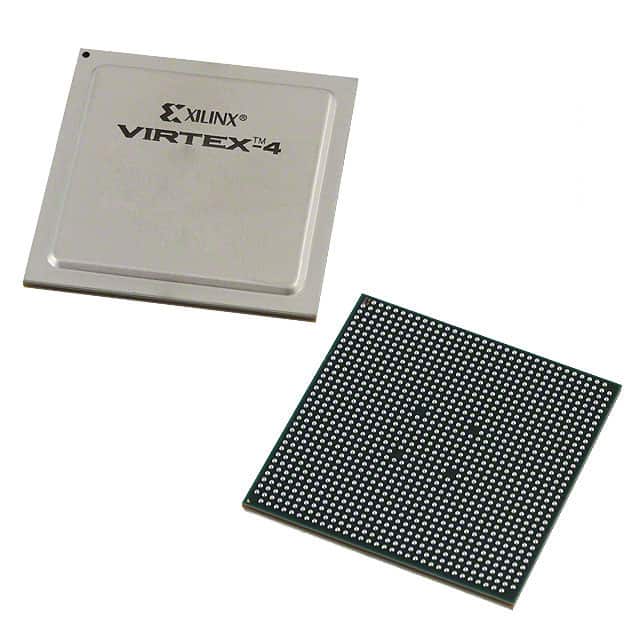
Package
XC2VP50-6FFG1148C is available in a Flip-Chip Fine-Pitch Ball Grid Array (FFGBA) package.
Essence
The essence of XC2VP50-6FFG1148C lies in its ability to provide a versatile and customizable solution for complex digital circuit designs.
Packaging/Quantity
XC2VP50-6FFG1148C is typically packaged individually and is available in varying quantities depending on customer requirements.
Specifications
- FPGA Family: Virtex-II Pro
- Logic Cells: 50,000
- System Gates: 1.5 million
- Number of I/Os: 1,148
- Operating Voltage: 1.2V
- Maximum Frequency: 500 MHz
- Embedded Block RAM: 4,608 Kbits
- DSP Slices: 192
- Configuration Memory: 36 Mb
- Package Type: FFGBA
- Temperature Range: -40°C to +100°C
Detailed Pin Configuration
The detailed pin configuration of XC2VP50-6FFG1148C can be found in the product datasheet provided by the manufacturer.
Functional Features
- High-speed serial connectivity
- On-chip PowerPC processor cores
- Built-in digital signal processing (DSP) capabilities
- Configurable I/O standards
- Embedded memory blocks for efficient data storage
- Flexible clock management resources
- Support for partial reconfiguration
Advantages and Disadvantages
Advantages
- Versatile and customizable design
- High-performance and high-speed data processing capabilities
- Low power consumption compared to traditional ASICs
- Support for various communication protocols
- Reconfigurable nature allows for flexibility in design changes
Disadvantages
- Higher cost compared to traditional fixed-function integrated circuits
- Steeper learning curve for designers due to complexity
- Limited availability of alternative models with similar specifications
Working Principles
XC2VP50-6FFG1148C operates based on the principles of FPGA technology. It consists of a large number of programmable logic cells interconnected through configurable routing resources. These logic cells can be programmed to implement desired digital circuit functionality. The configuration of the FPGA is stored in non-volatile memory, allowing it to retain its programmed state even after power is removed.
During operation, input signals are processed by the logic cells according to the programmed configuration, and the output signals are generated accordingly. The flexible nature of FPGAs enables designers to modify and reconfigure the circuit as needed, making them suitable for a wide range of applications.
Detailed Application Field Plans
XC2VP50-6FFG1148C finds extensive application in various fields, including:
- Telecommunications: Used in base stations, routers, and network switches for high-speed data processing and protocol handling.
- Automotive: Employed in advanced driver assistance systems (ADAS), infotainment systems, and engine control units (ECUs) for enhanced performance and functionality.
- Aerospace: Utilized in satellite communication systems, avionics, and radar systems for reliable and efficient data processing.
- Consumer Electronics: Integrated into high-definition televisions, gaming consoles, and multimedia devices for improved graphics processing and multimedia capabilities.
Detailed and Complete Alternative Models
While XC2VP50-6FFG1148C is a highly capable FPGA, there are alternative models available in the market with similar specifications. Some notable alternatives include:
- Xilinx Virtex-7 XC7VX485T-2FFG1761C
- Altera Stratix V 5SGXEA7N2F45C2LN
- Lattice Semiconductor ECP5-85
- Microsemi SmartFusion2 M2S050T-1FGG484I
These alternative models offer comparable performance and features, providing designers with options based on their specific requirements.
In conclusion, XC2VP50-6FFG1148C is a powerful FPGA that offers high-performance, flexibility, and versatility for various digital circuit applications. Its advanced features, extensive pin configuration, and functional capabilities make it a preferred choice in industries such as telecommunications, automotive, aerospace, and consumer electronics. While it has certain disadvantages, its
Noem 10 veelgestelde vragen en antwoorden met betrekking tot de toepassing van XC2VP50-6FFG1148C in technische oplossingen
Sure! Here are 10 common questions and answers related to the application of XC2VP50-6FFG1148C in technical solutions:
Question: What is XC2VP50-6FFG1148C?
- Answer: XC2VP50-6FFG1148C is a specific model of Field Programmable Gate Array (FPGA) manufactured by Xilinx.Question: What are the key features of XC2VP50-6FFG1148C?
- Answer: Some key features of XC2VP50-6FFG1148C include 50,000 logic cells, 6ns maximum delay, 1.2V core voltage, and 1.5V I/O voltage.Question: In what applications can XC2VP50-6FFG1148C be used?
- Answer: XC2VP50-6FFG1148C can be used in various applications such as telecommunications, networking, industrial automation, medical devices, and aerospace.Question: What is the maximum operating frequency of XC2VP50-6FFG1148C?
- Answer: The maximum operating frequency of XC2VP50-6FFG1148C is typically around 200 MHz.Question: Can XC2VP50-6FFG1148C be reprogrammed after deployment?
- Answer: Yes, XC2VP50-6FFG1148C is a field-programmable device, which means it can be reprogrammed even after it has been deployed in a system.Question: What development tools are available for programming XC2VP50-6FFG1148C?
- Answer: Xilinx provides software tools like Vivado Design Suite that can be used for designing, programming, and debugging XC2VP50-6FFG1148C.Question: What is the power consumption of XC2VP50-6FFG1148C?
- Answer: The power consumption of XC2VP50-6FFG1148C depends on the specific design and configuration, but it typically ranges from a few watts to tens of watts.Question: Can XC2VP50-6FFG1148C interface with other components or devices?
- Answer: Yes, XC2VP50-6FFG1148C supports various interfaces such as PCIe, Ethernet, USB, SPI, I2C, and more, allowing it to communicate with other components or devices in a system.Question: Are there any limitations or considerations when using XC2VP50-6FFG1148C?
- Answer: Some considerations include power supply requirements, thermal management, and ensuring proper signal integrity for high-speed designs.Question: Where can I find more information about XC2VP50-6FFG1148C?
- Answer: You can refer to the Xilinx website, datasheets, application notes, or consult with Xilinx representatives for more detailed information about XC2VP50-6FFG1148C.