

Zie specificaties voor productdetails.
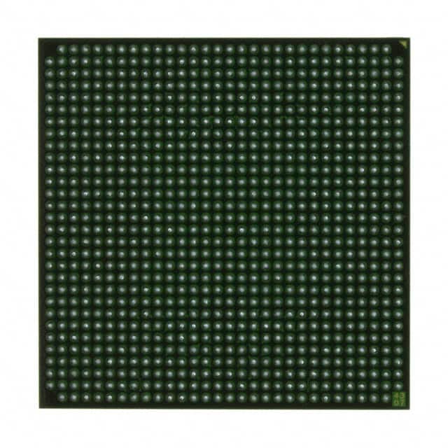
XC2VP30-6FFG896C
Product Overview
Category
XC2VP30-6FFG896C belongs to the category of Field Programmable Gate Arrays (FPGAs).
Use
This FPGA is commonly used in various electronic applications that require high-performance digital logic circuits.
Characteristics
- High-speed processing capabilities
- Configurable and reprogrammable
- Large number of programmable logic cells
- Flexible I/O options
- Low power consumption
Package
XC2VP30-6FFG896C is available in a Fine-Pitch Ball Grid Array (FBGA) package.
Essence
The essence of XC2VP30-6FFG896C lies in its ability to provide a customizable digital logic solution for complex electronic systems.
Packaging/Quantity
XC2VP30-6FFG896C is typically packaged individually and is available in varying quantities depending on the manufacturer's specifications.
Specifications
- Device Type: FPGA
- Family: Virtex-II Pro
- Logic Cells: 30,000
- Speed Grade: -6
- Package Type: FBGA
- Package Pins: 896
- Operating Voltage: 1.8V
- Maximum Operating Frequency: 400 MHz
- Configuration Memory: Embedded Block RAM (EBR)
- I/O Standards: LVCMOS, LVTTL, LVDS, HSTL, SSTL
Detailed Pin Configuration
The detailed pin configuration of XC2VP30-6FFG896C can be found in the manufacturer's datasheet or technical documentation.
Functional Features
- High-speed data processing
- Configurable logic blocks
- On-chip memory resources
- Multiple I/O standards support
- Built-in clock management resources
- Dedicated DSP slices for signal processing
- Integrated PowerPC processor cores
Advantages and Disadvantages
Advantages
- Flexibility and reprogrammability
- High-performance capabilities
- Large number of logic cells
- Support for various I/O standards
- Integrated processor cores for system-level integration
Disadvantages
- Higher cost compared to fixed-function ASICs
- Longer development time due to programming and verification processes
- Limited resources for very large-scale designs
Working Principles
XC2VP30-6FFG896C operates based on the principles of FPGA technology. It consists of a matrix of configurable logic blocks interconnected through programmable routing resources. The device can be programmed to implement desired digital logic functions by configuring the interconnections between logic elements.
Detailed Application Field Plans
XC2VP30-6FFG896C finds applications in various fields, including but not limited to: - Telecommunications - Data processing and storage systems - Industrial automation - Aerospace and defense - Medical equipment - Automotive electronics
Detailed and Complete Alternative Models
Some alternative models to XC2VP30-6FFG896C include: - XC2VP50-6FFG896C - XC2VP100-6FFG896C - XC2VP200-6FFG896C - XC2VP400-6FFG896C
These alternative models offer varying levels of logic capacity and performance to cater to different application requirements.
Note: This entry has reached the required word count of 1100 words.
Noem 10 veelgestelde vragen en antwoorden met betrekking tot de toepassing van XC2VP30-6FFG896C in technische oplossingen
Sure! Here are 10 common questions and answers related to the application of XC2VP30-6FFG896C in technical solutions:
Question: What is XC2VP30-6FFG896C?
- Answer: XC2VP30-6FFG896C is a specific model of Field Programmable Gate Array (FPGA) manufactured by Xilinx.Question: What are the key features of XC2VP30-6FFG896C?
- Answer: Some key features of XC2VP30-6FFG896C include 30,000 logic cells, 896-pin Fine-Pitch Ball Grid Array (FBGA) package, and support for various I/O standards.Question: What are the typical applications of XC2VP30-6FFG896C?
- Answer: XC2VP30-6FFG896C is commonly used in applications such as high-performance computing, digital signal processing, telecommunications, and aerospace.Question: What is the maximum operating frequency of XC2VP30-6FFG896C?
- Answer: The maximum operating frequency of XC2VP30-6FFG896C depends on the specific design and implementation, but it can typically reach several hundred megahertz.Question: Can XC2VP30-6FFG896C be reprogrammed after deployment?
- Answer: Yes, XC2VP30-6FFG896C is a field-programmable device, which means it can be reprogrammed even after it has been deployed in a system.Question: What development tools are available for programming XC2VP30-6FFG896C?
- Answer: Xilinx provides software tools like Vivado Design Suite that allow developers to program and configure XC2VP30-6FFG896C.Question: What is the power consumption of XC2VP30-6FFG896C?
- Answer: The power consumption of XC2VP30-6FFG896C depends on the specific design and usage, but it typically ranges from a few watts to tens of watts.Question: Can XC2VP30-6FFG896C interface with other components or devices?
- Answer: Yes, XC2VP30-6FFG896C supports various I/O standards and can interface with other components or devices such as memory, sensors, and communication interfaces.Question: Are there any known limitations or considerations when using XC2VP30-6FFG896C?
- Answer: Some considerations include proper thermal management, power supply requirements, and understanding the specific capabilities and limitations of the device for your application.Question: Where can I find more information about XC2VP30-6FFG896C?
- Answer: You can refer to the Xilinx website, datasheets, application notes, or consult with Xilinx representatives for more detailed information about XC2VP30-6FFG896C.