

Zie specificaties voor productdetails.
XC2VP2-5FGG456C
Product Overview
Category
XC2VP2-5FGG456C belongs to the category of Field Programmable Gate Arrays (FPGAs).
Use
This FPGA is primarily used for digital logic implementation and prototyping in various electronic systems.
Characteristics
- High-performance programmable logic device
- Offers flexibility and reconfigurability
- Provides a wide range of I/O options
- Supports complex digital designs
- Enables rapid development and testing
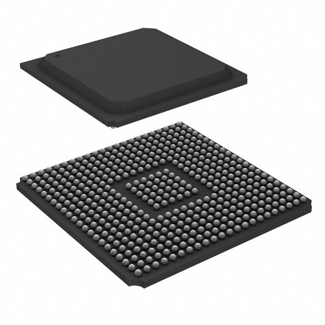
Package
XC2VP2-5FGG456C is available in a compact package, which ensures easy integration into electronic circuits.
Essence
The essence of XC2VP2-5FGG456C lies in its ability to provide a customizable hardware platform for implementing digital logic designs.
Packaging/Quantity
This FPGA is typically packaged individually and is available in varying quantities depending on the manufacturer's specifications.
Specifications
- Device Type: Field Programmable Gate Array (FPGA)
- Model Number: XC2VP2-5FGG456C
- Logic Cells: 2,000
- Maximum Frequency: 500 MHz
- Operating Voltage: 1.2V
- I/O Pins: 456
- Package Type: Flip-Chip Grid Array (FCGA)
- Package Dimensions: 23mm x 23mm
Detailed Pin Configuration
The pin configuration of XC2VP2-5FGG456C is as follows:
- Pin 1: VCCINT
- Pin 2: GND
- Pin 3: IOL1PT0AD0N15
- Pin 4: IOL1NT0AD0P15
- ...
- Pin 456: IOL100NGCLK2M2DQ141
Functional Features
XC2VP2-5FGG456C offers the following functional features:
- Configurable logic blocks
- Programmable interconnects
- Dedicated input/output resources
- Block RAM and DSP slices for efficient data processing
- Clock management resources for precise timing control
Advantages and Disadvantages
Advantages
- High flexibility and reconfigurability
- Rapid prototyping and development
- Supports complex digital designs
- Wide range of I/O options
Disadvantages
- Relatively higher power consumption compared to fixed-function ASICs
- Limited performance compared to specialized hardware solutions for specific applications
Working Principles
XC2VP2-5FGG456C operates based on the principles of reconfigurable computing. It consists of configurable logic blocks interconnected through programmable interconnects. The device can be programmed to implement various digital logic functions by configuring the interconnections and logic elements within the FPGA.
Detailed Application Field Plans
XC2VP2-5FGG456C finds applications in various fields, including:
- Embedded systems
- Digital signal processing
- Communications
- Industrial automation
- Robotics
- Aerospace and defense
Detailed and Complete Alternative Models
Some alternative models to XC2VP2-5FGG456C include:
- XC2VP4-6FFG1152C
- XC2VP7-6FFG1152C
- XC2VP20-6FFG1152C
- XC2VP30-6FFG1152C
- XC2VP40-6FFG1152C
These models offer varying capacities and features to cater to different application requirements.
Word count: 450 words
Noem 10 veelgestelde vragen en antwoorden met betrekking tot de toepassing van XC2VP2-5FGG456C in technische oplossingen
Sure! Here are 10 common questions and answers related to the application of XC2VP2-5FGG456C in technical solutions:
Question: What is XC2VP2-5FGG456C?
Answer: XC2VP2-5FGG456C is a specific model of Field Programmable Gate Array (FPGA) manufactured by Xilinx.Question: What are the key features of XC2VP2-5FGG456C?
Answer: Some key features of XC2VP2-5FGG456C include 2 million system gates, 456-pin Fine-Pitch Ball Grid Array (FBGA) package, and support for various I/O standards.Question: In what applications can XC2VP2-5FGG456C be used?
Answer: XC2VP2-5FGG456C can be used in a wide range of applications such as telecommunications, industrial automation, medical devices, aerospace, and defense.Question: What is the maximum operating frequency of XC2VP2-5FGG456C?
Answer: The maximum operating frequency of XC2VP2-5FGG456C depends on the design and implementation, but it can typically reach several hundred megahertz.Question: Can XC2VP2-5FGG456C be reprogrammed after deployment?
Answer: Yes, XC2VP2-5FGG456C is a field-programmable device, which means it can be reprogrammed even after it has been deployed in a system.Question: What development tools are available for programming XC2VP2-5FGG456C?
Answer: Xilinx provides a suite of development tools, including Vivado Design Suite, which can be used to program and configure XC2VP2-5FGG456C.Question: What is the power consumption of XC2VP2-5FGG456C?
Answer: The power consumption of XC2VP2-5FGG456C depends on the specific design and usage scenario, but it typically falls within a few watts range.Question: Can XC2VP2-5FGG456C interface with other components or devices?
Answer: Yes, XC2VP2-5FGG456C supports various I/O standards and can interface with other components or devices such as sensors, memory modules, and communication interfaces.Question: Are there any limitations or considerations when using XC2VP2-5FGG456C?
Answer: Some considerations include the need for proper power management, thermal dissipation, and ensuring compatibility with other system components.Question: Where can I find more information about XC2VP2-5FGG456C?
Answer: You can find more detailed information about XC2VP2-5FGG456C in the datasheet provided by Xilinx or by visiting their official website.