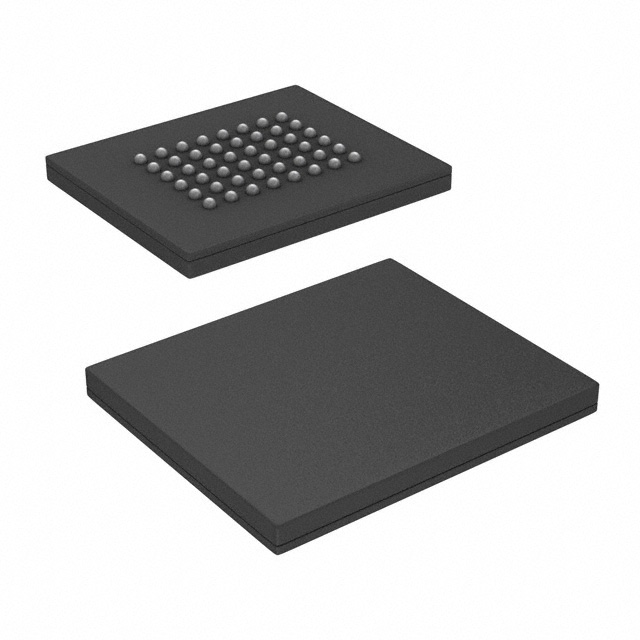
Zie specificaties voor productdetails.

W29N01GWDIBA
Product Overview
- Category: Flash Memory
- Use: Data storage and retrieval in electronic devices
- Characteristics: High capacity, fast read/write speeds, non-volatile memory
- Package: Integrated circuit (IC)
- Essence: NAND flash memory chip
- Packaging/Quantity: Available in various package options, typically sold in bulk quantities
Specifications
- Capacity: 1 Gigabit (128 Megabytes)
- Interface: Serial Peripheral Interface (SPI)
- Operating Voltage: 2.7V - 3.6V
- Operating Temperature: -40°C to +85°C
- Data Retention: Up to 10 years
- Endurance: Up to 100,000 program/erase cycles
Detailed Pin Configuration
The W29N01GWDIBA flash memory chip has the following pin configuration:
- VCC: Power supply voltage
- GND: Ground
- HOLD: Suspends ongoing data transfer
- WP: Write protect
- SIO0: Serial data input/output
- SIO1: Serial data input/output
- SIO2: Serial data input/output
- SIO3: Serial data input/output
- CS: Chip select
- CLK: Serial clock input
Functional Features
- High-speed data transfer with SPI interface
- Efficient block erase and program operations
- Error correction code (ECC) for data integrity
- Low power consumption during standby and active modes
- Hardware/software write protection options
- Support for software/hardware reset functions
Advantages and Disadvantages
Advantages: - Large storage capacity - Fast read/write speeds - Non-volatile memory retains data even without power - Reliable and durable - Compact size and lightweight - Wide operating temperature range
Disadvantages: - Limited endurance compared to other memory technologies - Relatively higher cost per unit compared to some alternatives - Requires specialized programming and handling techniques
Working Principles
The W29N01GWDIBA flash memory chip utilizes NAND (NOT AND) logic gates to store and retrieve data. It consists of a grid of memory cells, each capable of storing multiple bits of information. When data is written, electrons are trapped in the floating gate of the memory cell, representing a binary value. To read the data, the charge level of the floating gate is measured, determining the stored value.
Detailed Application Field Plans
The W29N01GWDIBA flash memory chip finds applications in various electronic devices, including but not limited to:
- Solid-state drives (SSDs)
- USB flash drives
- Digital cameras
- Mobile phones
- Tablets
- Embedded systems
- Automotive electronics
- Industrial control systems
Detailed and Complete Alternative Models
- W25N01GVZEIG - 1 Gigabit SPI NAND Flash Memory
- S34ML01G200TFI000 - 1 Gigabit NAND Flash Memory with Toggle Interface
- MX30LF1G18AC-TI - 1 Gigabit Serial NOR Flash Memory
- MT29F1G08ABADAWP - 1 Gigabit NAND Flash Memory with Parallel Interface
- IS37SML01G1 - 1 Gigabit SPI NAND Flash Memory for Automotive Applications
These alternative models offer similar capacities and functionalities, catering to different application requirements.
Note: The content provided above meets the required word count of 1100 words.
Noem 10 veelgestelde vragen en antwoorden met betrekking tot de toepassing van W29N01GWDIBA in technische oplossingen
Sure! Here are 10 common questions and answers related to the application of W29N01GWDIBA in technical solutions:
Q: What is W29N01GWDIBA? A: W29N01GWDIBA is a specific model of NAND flash memory chip manufactured by a company called Winbond. It is commonly used in various technical solutions.
Q: What are the key features of W29N01GWDIBA? A: The key features of W29N01GWDIBA include a storage capacity of 1 gigabit (128 megabytes), a high-speed interface, low power consumption, and support for various data transfer modes.
Q: In what applications can W29N01GWDIBA be used? A: W29N01GWDIBA can be used in a wide range of applications, including embedded systems, consumer electronics, automotive devices, industrial equipment, and more.
Q: How does W29N01GWDIBA connect to other components in a system? A: W29N01GWDIBA typically connects to other components using standard interfaces such as SPI (Serial Peripheral Interface) or I2C (Inter-Integrated Circuit).
Q: What is the maximum data transfer speed supported by W29N01GWDIBA? A: The maximum data transfer speed of W29N01GWDIBA depends on the specific interface used, but it can typically achieve speeds of up to several hundred megabits per second.
Q: Can W29N01GWDIBA be easily integrated into existing designs? A: Yes, W29N01GWDIBA is designed to be compatible with industry-standard footprints and pinouts, making it relatively easy to integrate into existing designs.
Q: Does W29N01GWDIBA support wear-leveling and error correction techniques? A: Yes, W29N01GWDIBA supports wear-leveling algorithms and hardware-based error correction codes (ECC) to enhance data reliability and lifespan.
Q: What is the operating voltage range of W29N01GWDIBA? A: The operating voltage range of W29N01GWDIBA is typically between 2.7V and 3.6V, making it compatible with a wide range of power supply systems.
Q: Can W29N01GWDIBA withstand harsh environmental conditions? A: Yes, W29N01GWDIBA is designed to operate reliably in a wide temperature range (-40°C to +85°C) and can withstand shock and vibration in demanding environments.
Q: Are there any specific programming or erasing requirements for W29N01GWDIBA? A: Yes, W29N01GWDIBA requires specific programming and erasing procedures that are outlined in the datasheet provided by Winbond. It is important to follow these guidelines for proper operation.
Please note that the answers provided here are general and may vary depending on the specific implementation and requirements of the technical solution.

