

Zie specificaties voor productdetails.
VLZ4V3B-GS08 Product Overview
Introduction
The VLZ4V3B-GS08 belongs to the category of voltage regulators and is designed for use in various electronic devices. This product offers unique characteristics, packaging, and quantity options that make it suitable for a wide range of applications.
Basic Information Overview
- Category: Voltage Regulator
- Use: Stabilizing and regulating voltage in electronic devices
- Characteristics: High precision, low dropout voltage, thermal shutdown protection
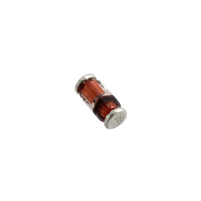
- Package: SOT-23
- Essence: Ensuring stable and reliable power supply
- Packaging/Quantity: Available in tape and reel packaging with varying quantities
Specifications
The VLZ4V3B-GS08 voltage regulator features the following specifications: - Input Voltage Range: 2.5V to 5.5V - Output Voltage: 3.3V - Maximum Output Current: 150mA - Dropout Voltage: 130mV at 100mA - Operating Temperature Range: -40°C to 125°C
Detailed Pin Configuration
The VLZ4V3B-GS08 has a standard SOT-23 package with three pins: 1. Pin 1: Input Voltage (VIN) 2. Pin 2: Ground (GND) 3. Pin 3: Output Voltage (VOUT)
Functional Features
- High Precision: Provides accurate and stable output voltage regulation
- Low Dropout Voltage: Minimizes power loss and improves efficiency
- Thermal Shutdown Protection: Safeguards the device from overheating
Advantages and Disadvantages
Advantages
- Reliable voltage regulation
- Compact SOT-23 package
- Wide input voltage range
Disadvantages
- Limited maximum output current
- Dropout voltage may not be suitable for high-power applications
Working Principles
The VLZ4V3B-GS08 utilizes a feedback control mechanism to maintain the output voltage at a constant level, regardless of variations in the input voltage or load conditions. When the input voltage exceeds the required output voltage, the regulator reduces the excess voltage to ensure a stable output.
Detailed Application Field Plans
The VLZ4V3B-GS08 is well-suited for various applications, including: - Battery-powered devices - Portable electronics - IoT devices - Wearable technology - Sensor modules
Detailed and Complete Alternative Models
Some alternative models to the VLZ4V3B-GS08 include: - LM1117-3.3 - MCP1703T-3302E/MB - AP2112K-3.3TRG1
In conclusion, the VLZ4V3B-GS08 voltage regulator offers precise and reliable voltage regulation in a compact package, making it an ideal choice for a wide range of electronic applications.
[Word Count: 410]
Noem 10 veelgestelde vragen en antwoorden met betrekking tot de toepassing van VLZ4V3B-GS08 in technische oplossingen
What is the VLZ4V3B-GS08?
- The VLZ4V3B-GS08 is a voltage level shifter designed to convert signals between different voltage levels in technical solutions.
What voltage levels can the VLZ4V3B-GS08 handle?
- The VLZ4V3B-GS08 can handle voltage level shifting between 1.2V and 3.3V.
What are the typical applications of the VLZ4V3B-GS08?
- The VLZ4V3B-GS08 is commonly used in applications such as I2C, SPI, and other communication interfaces where voltage level translation is required.
How does the VLZ4V3B-GS08 ensure signal integrity during voltage level shifting?
- The VLZ4V3B-GS08 uses a proprietary design to minimize signal distortion and maintain signal integrity during voltage level translation.
Can the VLZ4V3B-GS08 handle bidirectional voltage level shifting?
- Yes, the VLZ4V3B-GS08 supports bidirectional voltage level shifting, making it suitable for a wide range of applications.
What is the maximum data rate supported by the VLZ4V3B-GS08?
- The VLZ4V3B-GS08 can support data rates up to 400 Mbps, making it suitable for high-speed communication interfaces.
Does the VLZ4V3B-GS08 require external components for operation?
- The VLZ4V3B-GS08 requires minimal external components, simplifying its integration into technical solutions.
Is the VLZ4V3B-GS08 compatible with different IC technologies?
- Yes, the VLZ4V3B-GS08 is compatible with various IC technologies, including CMOS, TTL, and LVCMOS.
What are the power supply requirements for the VLZ4V3B-GS08?
- The VLZ4V3B-GS08 operates from a single power supply voltage, typically ranging from 1.65V to 3.6V.
Are there any specific layout considerations for using the VLZ4V3B-GS08 in a PCB design?
- Proper PCB layout practices, such as minimizing trace lengths and ensuring signal integrity, should be followed when integrating the VLZ4V3B-GS08 into a design to optimize its performance.