

Zie specificaties voor productdetails.
XC6108C40BGR-G
Product Overview
Category
XC6108C40BGR-G belongs to the category of voltage regulators.
Use
It is primarily used for regulating voltage in electronic circuits.
Characteristics
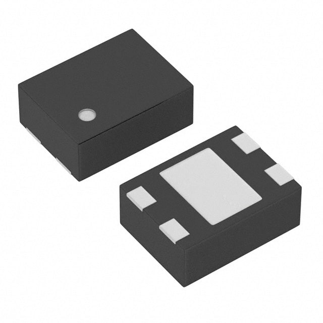
- Package: BGA (Ball Grid Array)
- Essence: Voltage regulator
- Packaging/Quantity: Typically sold in reels or trays, with a quantity of 1000 units per reel/tray.
Specifications
The specifications of XC6108C40BGR-G are as follows:
- Input Voltage Range: 2.5V - 6.0V
- Output Voltage: 4.0V
- Output Current: Up to 150mA
- Dropout Voltage: 200mV (typical)
- Quiescent Current: 30μA (typical)
- Operating Temperature Range: -40°C to +85°C
Detailed Pin Configuration
XC6108C40BGR-G has the following pin configuration:
- VIN: Input voltage pin
- GND: Ground pin
- EN: Enable pin
- VOUT: Output voltage pin
- CE: Capacitor connection pin for stability enhancement
Functional Features
The functional features of XC6108C40BGR-G include:
- Low dropout voltage for efficient regulation
- Low quiescent current for power-saving operation
- Built-in overcurrent protection
- Thermal shutdown protection
- Short-circuit protection
Advantages and Disadvantages
Advantages: - Compact BGA package for space-constrained applications - Wide input voltage range allows flexibility in design - Low quiescent current minimizes power consumption - Built-in protection features enhance reliability
Disadvantages: - Limited output current may not be suitable for high-power applications - BGA package requires specialized manufacturing techniques
Working Principles
XC6108C40BGR-G operates based on the principle of voltage regulation. It takes an input voltage within the specified range and provides a stable output voltage of 4.0V, even when the input voltage fluctuates.
The device uses internal circuitry to regulate the voltage and maintain a constant output, compensating for changes in load and input voltage. It achieves this through a combination of feedback control and power transistor switching.
Detailed Application Field Plans
XC6108C40BGR-G finds applications in various electronic devices and systems, including but not limited to:
- Battery-powered devices: Portable electronics, handheld instruments, etc.
- IoT (Internet of Things) devices: Sensors, smart home devices, wearable technology, etc.
- Automotive electronics: Infotainment systems, navigation systems, etc.
- Industrial equipment: Control systems, measurement devices, etc.
- Communication devices: Wireless routers, access points, etc.
Detailed and Complete Alternative Models
Some alternative models that can be considered as alternatives to XC6108C40BGR-G are:
- XC6206P332MR-G: A 3.3V voltage regulator with similar characteristics and package.
- XC6220B331MR-G: A 3.3V voltage regulator with lower dropout voltage and higher output current.
- XC6219B332MR-G: A 3.3V voltage regulator with additional protection features.
These alternative models provide options with different specifications and features, allowing designers to choose the most suitable voltage regulator for their specific application requirements.
Word count: 445 words
Noem 10 veelgestelde vragen en antwoorden met betrekking tot de toepassing van XC6108C40BGR-G in technische oplossingen
Sure! Here are 10 common questions and answers related to the application of XC6108C40BGR-G in technical solutions:
Q: What is XC6108C40BGR-G? A: XC6108C40BGR-G is a voltage detector IC (integrated circuit) that monitors the power supply voltage and provides a reset signal when the voltage drops below a certain threshold.
Q: What is the operating voltage range of XC6108C40BGR-G? A: The operating voltage range of XC6108C40BGR-G is typically between 0.9V and 6.0V.
Q: How does XC6108C40BGR-G help in technical solutions? A: XC6108C40BGR-G helps in technical solutions by ensuring proper system operation and preventing data corruption or malfunctioning due to low voltage conditions.
Q: Can XC6108C40BGR-G be used in battery-powered applications? A: Yes, XC6108C40BGR-G can be used in battery-powered applications as it has a low quiescent current consumption of typically 1.0µA.
Q: What is the output type of XC6108C40BGR-G? A: XC6108C40BGR-G has an open-drain output type, which allows for flexibility in connecting to different microcontrollers or devices.
Q: What is the typical reset threshold voltage of XC6108C40BGR-G? A: The typical reset threshold voltage of XC6108C40BGR-G is 4.0V.
Q: Does XC6108C40BGR-G have a built-in delay time for the reset signal? A: Yes, XC6108C40BGR-G has a built-in delay time of typically 200ms to ensure stable power supply before releasing the reset signal.
Q: Can XC6108C40BGR-G be used in automotive applications? A: Yes, XC6108C40BGR-G is suitable for automotive applications as it meets the AEC-Q100 Grade 2 qualification standards.
Q: What is the package type of XC6108C40BGR-G? A: XC6108C40BGR-G is available in a small SOT-25 package, which is compact and space-saving.
Q: Where can I find more information about XC6108C40BGR-G? A: You can find more detailed information about XC6108C40BGR-G in the datasheet provided by the manufacturer or on their official website.