

Zie specificaties voor productdetails.
SN74LVC1G79YEAR
Product Overview
- Category: Integrated Circuit (IC)
- Use: Logic Gate
- Characteristics: Single Positive Edge-Triggered D-Type Flip-Flop
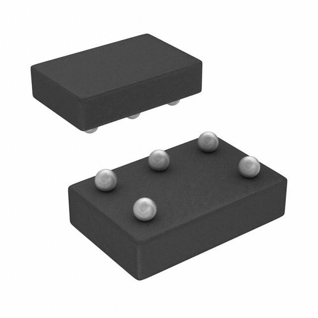
- Package: SOT-23-5
- Essence: High-speed CMOS technology
- Packaging/Quantity: Tape and Reel, 3000 pieces per reel
Specifications
- Supply Voltage Range: 1.65V to 5.5V
- High-Speed Operation: 20 ns maximum propagation delay
- Low Power Consumption: ICC = 2 μA maximum
- Operating Temperature Range: -40°C to +125°C
Detailed Pin Configuration
The SN74LVC1G79YEAR has a total of 5 pins:
- GND (Ground): Connected to the ground reference potential.
- Q (Output): Output of the flip-flop, representing the stored data.
- D (Data Input): Input for the data to be stored in the flip-flop.
- CLK (Clock Input): Clock signal input that triggers the flip-flop.
- VCC (Power Supply): Connected to the positive supply voltage.
Functional Features
- Single positive edge-triggered D-type flip-flop with asynchronous clear functionality.
- The flip-flop stores the data at the rising edge of the clock signal.
- Asynchronous clear input allows resetting the flip-flop to a known state.
- High-speed operation enables quick data storage and retrieval.
- Low power consumption makes it suitable for battery-powered devices.
Advantages and Disadvantages
Advantages: - Compact size and low pin count make it suitable for space-constrained applications. - Wide supply voltage range allows compatibility with various systems. - High-speed operation ensures efficient data processing. - Low power consumption prolongs battery life in portable devices.
Disadvantages: - Limited functionality compared to more complex flip-flops. - Single flip-flop may not be sufficient for certain applications requiring multiple storage elements.
Working Principles
The SN74LVC1G79YEAR is a positive edge-triggered D-type flip-flop. It stores the data present at the D input when a rising edge is detected on the CLK input. The stored data appears at the Q output and remains unchanged until the next clock pulse. The asynchronous clear input (CLR) resets the flip-flop to a known state, regardless of the clock signal.
Detailed Application Field Plans
The SN74LVC1G79YEAR can be used in various applications, including but not limited to: - Digital communication systems - Data storage devices - Microcontrollers and microprocessors - Consumer electronics - Automotive electronics - Industrial control systems
Detailed and Complete Alternative Models
Some alternative models that offer similar functionality to the SN74LVC1G79YEAR are: - MC74VHC1G79: High-Speed CMOS Logic Flip-Flop - 74AHC1G79: Single Positive Edge-Triggered D-Type Flip-Flop - CD4013B: Dual D-Type Flip-Flop
These alternative models provide different package options, supply voltage ranges, and additional features while serving the same purpose as the SN74LVC1G79YEAR.
Word count: 320 words
Noem 10 veelgestelde vragen en antwoorden met betrekking tot de toepassing van SN74LVC1G79YEAR in technische oplossingen
Sure! Here are 10 common questions and answers related to the application of SN74LVC1G79YEAR in technical solutions:
Q1: What is SN74LVC1G79YEAR? A1: SN74LVC1G79YEAR is a single positive-edge-triggered D-type flip-flop with clear, designed for 1.65-V to 5.5-V VCC operation.
Q2: What is the purpose of SN74LVC1G79YEAR? A2: SN74LVC1G79YEAR is used to store a single bit of data in digital circuits. It can be used for various applications such as synchronization, data storage, and signal delay.
Q3: What is the voltage range supported by SN74LVC1G79YEAR? A3: SN74LVC1G79YEAR supports a voltage range from 1.65V to 5.5V, making it compatible with a wide range of digital systems.
Q4: How many inputs and outputs does SN74LVC1G79YEAR have? A4: SN74LVC1G79YEAR has one data input (D), one clock input (CLK), one clear input (CLR), and one output (Q).
Q5: What is the maximum clock frequency supported by SN74LVC1G79YEAR? A5: SN74LVC1G79YEAR can operate at a maximum clock frequency of 100 MHz, allowing for high-speed data processing.
Q6: Can SN74LVC1G79YEAR be cascaded to create larger memory storage? A6: Yes, multiple SN74LVC1G79YEAR flip-flops can be cascaded together to create larger memory storage by connecting the output (Q) of one flip-flop to the input (D) of the next.
Q7: Does SN74LVC1G79YEAR have any built-in protection features? A7: Yes, SN74LVC1G79YEAR has built-in protection features such as overvoltage tolerance and undervoltage lockout, which help safeguard the device from voltage fluctuations.
Q8: What is the power supply current consumption of SN74LVC1G79YEAR? A8: The power supply current consumption of SN74LVC1G79YEAR is typically around 2.5 mA, making it suitable for low-power applications.
Q9: Can SN74LVC1G79YEAR be used in both digital and analog circuits? A9: No, SN74LVC1G79YEAR is specifically designed for digital circuits and is not recommended for use in analog applications.
Q10: Are there any specific layout considerations for using SN74LVC1G79YEAR? A10: Yes, it is important to follow the recommended layout guidelines provided in the datasheet to ensure proper signal integrity and minimize noise interference.
Please note that these answers are general and may vary depending on the specific application and requirements. It is always recommended to refer to the datasheet and consult with technical experts for accurate information.