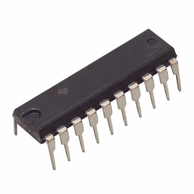
Zie specificaties voor productdetails.

CY74FCT374ATPC
Product Overview
- Category: Integrated Circuit (IC)
- Use: Flip-Flop
- Characteristics: High-speed, low-power, octal D-type flip-flop
- Package: 20-pin TSSOP (Thin Shrink Small Outline Package)
- Essence: Sequential logic device used for storing and transferring data
- Packaging/Quantity: Available in reels of 2500 units
Specifications
- Supply Voltage Range: 4.5V to 5.5V
- Input Voltage Range: 0V to VCC
- Output Voltage Range: 0V to VCC
- Operating Temperature Range: -40°C to +85°C
- Propagation Delay Time: 3.5ns (typical)
- Output Drive Capability: ±24mA
Pin Configuration
The CY74FCT374ATPC has a total of 20 pins, which are assigned specific functions as follows:
- Q0: Output of Flip-Flop 0
- D0: Data input for Flip-Flop 0
- CP: Clock input for Flip-Flops
- OE: Output Enable input
- GND: Ground
- Q7: Output of Flip-Flop 7
- D7: Data input for Flip-Flop 7
- Q6: Output of Flip-Flop 6
- D6: Data input for Flip-Flop 6
- Q5: Output of Flip-Flop 5
- D5: Data input for Flip-Flop 5
- Q4: Output of Flip-Flop 4
- D4: Data input for Flip-Flop 4
- VCC: Power supply voltage
- Q3: Output of Flip-Flop 3
- D3: Data input for Flip-Flop 3
- Q2: Output of Flip-Flop 2
- D2: Data input for Flip-Flop 2
- Q1: Output of Flip-Flop 1
- D1: Data input for Flip-Flop 1
Functional Features
- High-speed operation allows for efficient data transfer.
- Low-power consumption makes it suitable for battery-powered devices.
- Octal design enables the storage and transfer of eight bits of data simultaneously.
- Output Enable (OE) input allows for easy control of output states.
Advantages and Disadvantages
Advantages: - High-speed operation ensures quick data processing. - Low-power consumption extends battery life in portable devices. - Octal design provides efficient handling of multiple data bits. - Output Enable input offers flexibility in controlling output states.
Disadvantages: - Limited to a specific package type (TSSOP). - Requires external clock signal for proper functioning.
Working Principles
The CY74FCT374ATPC is an octal D-type flip-flop that operates on the rising edge of the clock signal (CP). When the clock input transitions from low to high, the data present at the D0-D7 inputs is transferred to the corresponding Q0-Q7 outputs. The Output Enable (OE) input controls the state of the outputs, allowing them to be enabled or disabled as required.
Detailed Application Field Plans
The CY74FCT374ATPC is commonly used in various digital systems and applications, including:
- Microprocessors and microcontrollers
- Data storage systems
- Communication equipment
- Industrial automation
- Automotive electronics
- Consumer electronics
Alternative Models
Here are some alternative models that offer similar functionality to the CY74FCT374ATPC:
- SN74F374: Texas Instruments
- MC74F374: ON Semiconductor
- 74FCT374: Integrated Device Technology (IDT)
- CD74FCT374: Texas Instruments
These alternative models can be considered based on specific requirements and availability.
In conclusion, the CY74FCT374ATPC is a high-speed, low-power octal D-type flip-flop IC. It offers efficient data storage and transfer capabilities, making it suitable for various digital applications. With its compact TSSOP package and reliable performance, it serves as a key component in many electronic systems.
Noem 10 veelgestelde vragen en antwoorden met betrekking tot de toepassing van CY74FCT374ATPC in technische oplossingen
Sure! Here are 10 common questions and answers related to the application of CY74FCT374ATPC in technical solutions:
Q: What is the CY74FCT374ATPC? A: The CY74FCT374ATPC is a type of octal D-type flip-flop integrated circuit (IC) that can store and transfer data in digital systems.
Q: What is the purpose of the CY74FCT374ATPC? A: The purpose of this IC is to provide a means of storing and transferring data within a digital system, making it useful for applications such as data storage, buffering, and synchronization.
Q: How many flip-flops are there in the CY74FCT374ATPC? A: The CY74FCT374ATPC contains eight individual D-type flip-flops, allowing it to store and manipulate up to eight bits of data.
Q: What is the operating voltage range for the CY74FCT374ATPC? A: The operating voltage range for this IC typically ranges from 4.5V to 5.5V, making it compatible with standard TTL logic levels.
Q: Can the CY74FCT374ATPC be used in both synchronous and asynchronous applications? A: Yes, the CY74FCT374ATPC can be used in both synchronous and asynchronous applications, depending on the specific requirements of the system.
Q: What is the maximum clock frequency supported by the CY74FCT374ATPC? A: The maximum clock frequency supported by this IC is typically around 100 MHz, although the exact value may vary depending on the specific operating conditions.
Q: Does the CY74FCT374ATPC have any built-in output enable functionality? A: Yes, the CY74FCT374ATPC includes a built-in output enable (OE) pin that can be used to control the output state of the flip-flops.
Q: Can the CY74FCT374ATPC be cascaded to increase the number of stored bits? A: Yes, multiple CY74FCT374ATPC ICs can be cascaded together to increase the number of stored bits in a digital system.
Q: What is the typical power consumption of the CY74FCT374ATPC? A: The typical power consumption of this IC is relatively low, typically ranging from a few milliwatts to a few hundred milliwatts, depending on the operating conditions.
Q: Are there any specific precautions or considerations when using the CY74FCT374ATPC? A: It is important to ensure proper decoupling and power supply bypassing for stable operation. Additionally, attention should be given to signal integrity, clock skew, and setup/hold time requirements when designing with this IC.

