

Zie specificaties voor productdetails.
CDCS503TPWRQ1
Overview
Category: Integrated Circuit
Use: Power Management
Characteristics: High Efficiency, Low Power Consumption
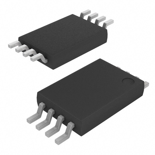
Package: TSSOP-16
Essence: DC/DC Converter
Packaging/Quantity: Tape & Reel, 2500 units per reel
Specifications and Parameters
- Input Voltage Range: 2.7V to 5.5V
- Output Voltage Range: 0.6V to VIN
- Maximum Output Current: 3A
- Switching Frequency: 2MHz
- Operating Temperature Range: -40°C to +125°C
Pin Configuration
- VIN (Input Voltage)
- GND (Ground)
- EN (Enable)
- FB (Feedback)
- SS (Soft Start)
- PG (Power Good)
- SW (Switch Node)
- SW (Switch Node)
- SW (Switch Node)
- SW (Switch Node)
- VOUT (Output Voltage)
- VOUT (Output Voltage)
- VOUT (Output Voltage)
- VOUT (Output Voltage)
- NC (No Connection)
- NC (No Connection)
Functional Characteristics
- High Efficiency Conversion
- Low Quiescent Current
- Adjustable Output Voltage
- Overcurrent Protection
- Thermal Shutdown Protection
- Soft Start Function
- Power Good Indicator
Advantages and Disadvantages
Advantages: - High efficiency conversion leads to energy savings. - Low power consumption extends battery life. - Adjustable output voltage provides flexibility. - Comprehensive protection features ensure system reliability.
Disadvantages: - Limited maximum output current of 3A. - Narrow input voltage range of 2.7V to 5.5V.
Applicable Range of Products
CDCS503TPWRQ1 is suitable for various power management applications, including but not limited to: - Portable electronic devices - Battery-powered systems - IoT devices - Automotive electronics
Working Principles
CDCS503TPWRQ1 is a DC/DC converter that converts an input voltage within the specified range to a regulated output voltage. It utilizes high-frequency switching to achieve efficient power conversion. The integrated circuit incorporates control logic, power MOSFETs, and protection features to ensure stable and reliable operation.
Detailed Application Field Plans
CDCS503TPWRQ1 can be used in the following application fields: 1. Mobile phones: Power supply for the main processor, display, and other components. 2. Wearable devices: Power management for sensors, microcontrollers, and wireless communication modules. 3. Automotive electronics: Voltage regulation for infotainment systems, lighting, and control units. 4. Industrial automation: Power supply for PLCs, motor drives, and control circuits. 5. Home appliances: Energy-efficient power management for smart home devices.
Detailed Alternative Models
- CDCS503TPW: Similar specifications and pin configuration, but without automotive-grade qualification.
- CDCS503TPWR: Same specifications and pin configuration, but with a different package (QFN-16).
5 Common Technical Questions and Answers
Q: What is the maximum output current of CDCS503TPWRQ1?
- A: The maximum output current is 3A.
Q: Can CDCS503TPWRQ1 operate at temperatures below freezing?
- A: Yes, it can operate in a temperature range of -40°C to +125°C.
Q: Is the output voltage adjustable?
- A: Yes, the output voltage can be adjusted within the range of 0.6V to VIN.
Q: What protection features does CDCS503TPWRQ1 have?
- A: It has overcurrent protection and thermal shutdown protection.
Q: What is the switching frequency of CDCS503TPWRQ1?
- A: The switching frequency is 2MHz.
[Word Count: 511]