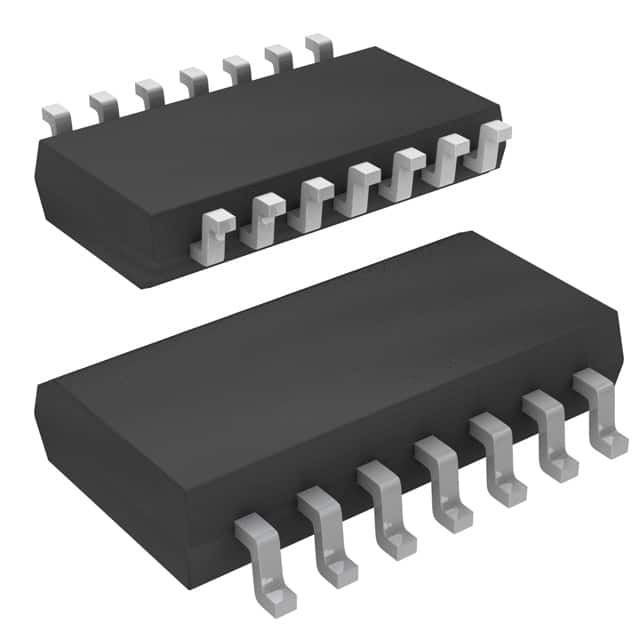
Zie specificaties voor productdetails.

CD4007UBNSRG4
Product Overview
- Category: Integrated Circuit
- Use: Logic Gate
- Characteristics: High Voltage, Low Power Consumption
- Package: SOIC (Small Outline Integrated Circuit)
- Essence: Complementary MOS (CMOS) Technology
- Packaging/Quantity: Tape and Reel, 2500 units per reel
Specifications
- Supply Voltage Range: 3V to 18V
- Input Voltage Range: -0.5V to VDD + 0.5V
- Output Voltage Range: -0.5V to VDD + 0.5V
- Operating Temperature Range: -55°C to +125°C
- Propagation Delay Time: 60ns (typical)
- Quiescent Current: 100µA (maximum)
Detailed Pin Configuration
The CD4007UBNSRG4 has a total of 14 pins, which are divided into two sections:
Section A
- Pin 1: VDD - Positive Power Supply
- Pin 2: GND - Ground
- Pin 3: Q1 - Output of Inverter 1
- Pin 4: Q2 - Output of Inverter 2
- Pin 5: Q3 - Output of Inverter 3
- Pin 6: Q4 - Output of Inverter 4
Section B
- Pin 7: VSS - Negative Power Supply
- Pin 8: A - Input of Inverter 1
- Pin 9: B - Input of Inverter 2
- Pin 10: C - Input of Inverter 3
- Pin 11: D - Input of Inverter 4
- Pin 12: Q5 - Output of Inverter 5
- Pin 13: Q6 - Output of Inverter 6
- Pin 14: VDD - Positive Power Supply
Functional Features
- Complementary MOS (CMOS) technology allows for high noise immunity and low power consumption.
- The CD4007UBNSRG4 consists of three pairs of complementary MOSFETs, which can be used as inverters or amplifiers.
- It offers a wide supply voltage range, making it suitable for various applications.
- The device has a high input impedance and low output impedance, ensuring compatibility with different logic families.
Advantages and Disadvantages
Advantages
- High noise immunity due to CMOS technology.
- Low power consumption.
- Wide supply voltage range.
- Versatile usage as inverters or amplifiers.
Disadvantages
- Relatively slower propagation delay compared to other logic gates.
- Limited current handling capability.
Working Principles
The CD4007UBNSRG4 utilizes complementary MOSFETs to perform logical operations. Each pair of MOSFETs acts as an inverter, where the input signal is inverted at the output. By connecting multiple inverters together, complex logic functions can be implemented.
Detailed Application Field Plans
The CD4007UBNSRG4 finds applications in various fields, including:
- Digital Electronics: Used in digital circuits for logic operations, such as signal inversion, buffering, and level shifting.
- Communication Systems: Employed in signal processing and modulation/demodulation circuits.
- Industrial Control Systems: Utilized in control logic circuits for automation and process control.
- Instrumentation: Integrated into measurement and data acquisition systems for signal conditioning and processing.
Detailed and Complete Alternative Models
- CD4001UB: Quad 2-input NOR gate
- CD4011UB: Quad 2-input NAND gate
- CD4013UB: Dual D-type flip-flop
- CD4017UB: Decade counter/divider with 10 decoded outputs
These alternative models offer similar functionality and can be used as substitutes for the CD4007UBNSRG4 in various applications.
Word count: 411 words
Noem 10 veelgestelde vragen en antwoorden met betrekking tot de toepassing van CD4007UBNSRG4 in technische oplossingen
Sure! Here are 10 common questions and answers related to the application of CD4007UBNSRG4:
Q: What is CD4007UBNSRG4?
A: CD4007UBNSRG4 is a CMOS integrated circuit that consists of three complementary pairs of MOS transistors.Q: What are the typical applications of CD4007UBNSRG4?
A: CD4007UBNSRG4 is commonly used in analog switching, waveform generation, voltage inversion, and other signal processing applications.Q: What is the supply voltage range for CD4007UBNSRG4?
A: The supply voltage range for CD4007UBNSRG4 is typically between 3V and 18V.Q: Can CD4007UBNSRG4 be used as a digital logic gate?
A: No, CD4007UBNSRG4 is primarily designed for analog applications and is not suitable for digital logic gate functions.Q: What is the maximum operating frequency of CD4007UBNSRG4?
A: The maximum operating frequency of CD4007UBNSRG4 is typically around 10 MHz.Q: How many channels does CD4007UBNSRG4 have?
A: CD4007UBNSRG4 has six independent channels, each consisting of a pair of complementary MOS transistors.Q: Can CD4007UBNSRG4 handle high currents?
A: No, CD4007UBNSRG4 is not designed to handle high currents. It is typically used for low-power applications.Q: Is CD4007UBNSRG4 sensitive to electrostatic discharge (ESD)?
A: Yes, CD4007UBNSRG4 is sensitive to ESD. Proper ESD precautions should be taken during handling and assembly.Q: Can CD4007UBNSRG4 operate in a wide temperature range?
A: Yes, CD4007UBNSRG4 is designed to operate in a wide temperature range, typically from -55°C to 125°C.Q: Are there any recommended reference designs or application notes available for CD4007UBNSRG4?
A: Yes, the manufacturer of CD4007UBNSRG4 provides datasheets, application notes, and reference designs that can help in understanding its usage and implementation in technical solutions.
Please note that these answers are general and may vary depending on specific datasheet specifications and application requirements.

