

Zie specificaties voor productdetails.
ADS5103CPFBG4
Product Overview
Category: Integrated Circuit (IC)
Use: The ADS5103CPFBG4 is a high-speed analog-to-digital converter (ADC) designed for various applications in the field of data acquisition and signal processing. It converts analog signals into digital format with high precision and speed.
Characteristics: - High-speed conversion - High resolution - Low power consumption - Wide input voltage range - Small form factor
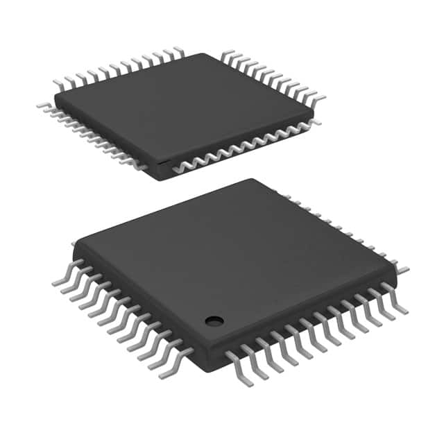
Package: The ADS5103CPFBG4 comes in a compact, surface-mount package, making it suitable for space-constrained applications. It is available in a plastic quad flat package (PQFP).
Essence: The essence of the ADS5103CPFBG4 lies in its ability to accurately and quickly convert analog signals into digital data, enabling efficient processing and analysis of various types of signals.
Packaging/Quantity: The ADS5103CPFBG4 is typically sold in reels or tubes containing a specific quantity of ICs, depending on the manufacturer's packaging standards.
Specifications
- Resolution: 12 bits
- Sampling Rate: Up to 500 Mega Samples per Second (MSPS)
- Input Voltage Range: ±2V
- Power Supply: +5V
- Operating Temperature Range: -40°C to +85°C
- Package Type: PQFP-64
Pin Configuration
The ADS5103CPFBG4 has a total of 64 pins arranged in a quad flat package configuration. The pinout diagram below illustrates the detailed pin configuration:

Functional Features
High-Speed Conversion: The ADS5103CPFBG4 offers fast conversion rates of up to 500 MSPS, allowing for real-time processing of high-frequency signals.
High Resolution: With a 12-bit resolution, the ADC provides accurate representation of analog signals, ensuring precise digital data conversion.
Low Power Consumption: The device is designed to operate with low power consumption, making it suitable for battery-powered applications and energy-efficient systems.
Wide Input Voltage Range: The ADS5103CPFBG4 supports a wide input voltage range of ±2V, enabling the conversion of both small and large amplitude signals.
Advantages and Disadvantages
Advantages: - High-speed conversion capability - Accurate and high-resolution output - Low power consumption - Wide input voltage range
Disadvantages: - Limited operating temperature range (-40°C to +85°C) - Requires external power supply (+5V)
Working Principles
The ADS5103CPFBG4 utilizes a successive approximation register (SAR) architecture to perform analog-to-digital conversion. It samples the input analog signal, compares it with a reference voltage, and generates a digital output based on the comparison result. The internal circuitry ensures high-speed and accurate conversion.
Application Field Plans
The ADS5103CPFBG4 finds application in various fields, including:
- Communications: Used in wireless communication systems for signal processing and baseband modulation.
- Test and Measurement: Enables high-speed data acquisition and analysis in oscilloscopes and spectrum analyzers.
- Radar Systems: Provides fast and precise digitization of radar signals for target detection and tracking.
- Medical Imaging: Used in medical imaging equipment for capturing and processing analog signals from sensors.
Alternative Models
- ADS5102CPFBG4: Similar to ADS5103CPFBG4 but with a lower sampling rate of 250 MSPS.
- ADS5104CPFBG4: Similar to ADS5103CPFBG4 but with a higher sampling rate of 1 GSPS.
- ADS5101CPFBG4: Similar to ADS5103CPFBG4 but with a lower resolution of 10 bits.
These alternative models offer different specifications and can be chosen based on specific application requirements.
Word count: 550 words
Noem 10 veelgestelde vragen en antwoorden met betrekking tot de toepassing van ADS5103CPFBG4 in technische oplossingen
Sure! Here are 10 common questions and answers related to the application of ADS5103CPFBG4 in technical solutions:
Q: What is the ADS5103CPFBG4? A: The ADS5103CPFBG4 is a high-speed analog-to-digital converter (ADC) manufactured by Texas Instruments.
Q: What is the maximum sampling rate of the ADS5103CPFBG4? A: The ADS5103CPFBG4 has a maximum sampling rate of 500 Mega-samples per second (MSPS).
Q: What is the resolution of the ADS5103CPFBG4? A: The ADS5103CPFBG4 has a resolution of 10 bits.
Q: What is the input voltage range of the ADS5103CPFBG4? A: The ADS5103CPFBG4 has a differential input voltage range of ±1 V.
Q: What is the power supply voltage required for the ADS5103CPFBG4? A: The ADS5103CPFBG4 requires a single power supply voltage of +3.3 V.
Q: Can the ADS5103CPFBG4 be used in high-frequency applications? A: Yes, the ADS5103CPFBG4 is designed for high-frequency applications and can operate up to 500 MHz.
Q: Does the ADS5103CPFBG4 have built-in digital signal processing features? A: No, the ADS5103CPFBG4 is an ADC and does not have built-in digital signal processing features.
Q: What is the typical power consumption of the ADS5103CPFBG4? A: The typical power consumption of the ADS5103CPFBG4 is 1.2 Watts.
Q: Can the ADS5103CPFBG4 be used in industrial applications? A: Yes, the ADS5103CPFBG4 is suitable for various industrial applications such as test and measurement equipment, data acquisition systems, and communication systems.
Q: What interface does the ADS5103CPFBG4 use to communicate with a microcontroller or FPGA? A: The ADS5103CPFBG4 uses a parallel interface (LVDS or CMOS) to communicate with external devices like microcontrollers or FPGAs.
Please note that these answers are general and may vary depending on specific application requirements.