

Zie specificaties voor productdetails.
ADC12DL040CIVSX
Product Overview
- Category: Analog-to-Digital Converter (ADC)
- Use: Converts analog signals into digital data for processing
- Characteristics: High-speed, high-resolution, low-power consumption
- Package: Integrated Circuit (IC)
- Essence: Converts continuous analog signals to discrete digital values
- Packaging/Quantity: Available in tape and reel packaging, quantity varies based on supplier
Specifications
- Resolution: 12 bits
- Sampling Rate: Up to 40 Mega Samples Per Second (MSPS)
- Input Voltage Range: 0V to VREF
- Power Supply: 3.3V
- Operating Temperature Range: -40°C to +85°C
- Interface: Serial Peripheral Interface (SPI)
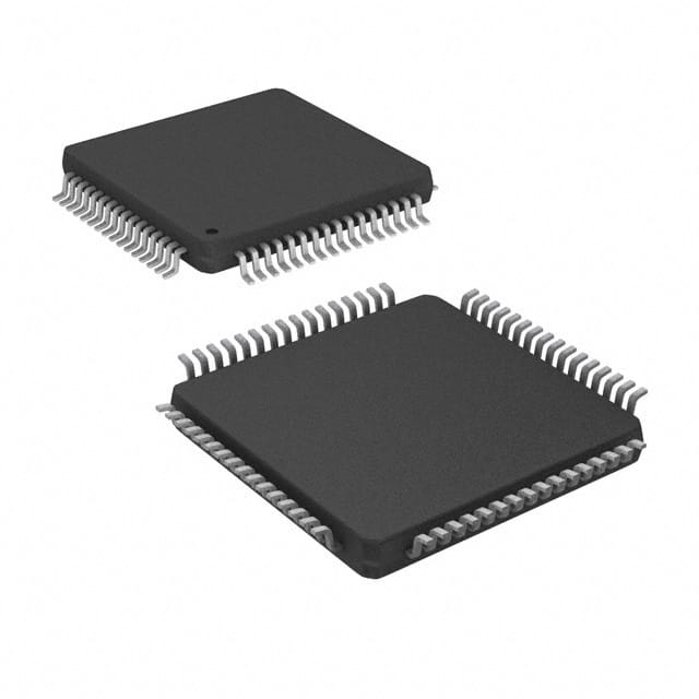
Pin Configuration
The ADC12DL040CIVSX has a total of 28 pins. The pin configuration is as follows:
- VREF-
- VREF+
- AGND
- AVDD
- DVDD
- DGND
- CLK
- CS
- SDATA
- SCLK
- DOUT
- DIN
- PDWN
- RESET
- REFSEL
- AIN0
- AIN1
- AIN2
- AIN3
- AIN4
- AIN5
- AIN6
- AIN7
- AIN8
- AIN9
- AIN10
- AIN11
- VIO
Functional Features
- High-speed conversion with a sampling rate of up to 40 MSPS
- 12-bit resolution provides accurate representation of analog signals
- Low-power consumption for energy-efficient operation
- Serial Peripheral Interface (SPI) allows easy integration with microcontrollers and other digital devices
- Wide input voltage range enables versatile signal processing
Advantages and Disadvantages
Advantages: - High-speed and high-resolution conversion - Low-power consumption - Versatile input voltage range - Easy integration with digital devices through SPI interface
Disadvantages: - Limited to 12-bit resolution, may not be suitable for applications requiring higher precision - Requires external power supply and reference voltage
Working Principles
The ADC12DL040CIVSX operates on the principle of successive approximation. It samples the analog input voltage and converts it into a digital value using an internal comparator and a digital-to-analog converter. The conversion process is controlled by an internal clock and the resulting digital data is transmitted through the SPI interface.
Detailed Application Field Plans
The ADC12DL040CIVSX finds applications in various fields, including:
- Communications: Used in wireless communication systems for signal processing and modulation/demodulation.
- Industrial Automation: Enables precise measurement and control in industrial automation systems.
- Medical Equipment: Provides accurate data acquisition in medical devices such as patient monitors and diagnostic equipment.
- Test and Measurement: Used in test and measurement instruments for accurate signal analysis and data acquisition.
- Audio Processing: Enables high-quality audio signal conversion in audio processing systems.
Detailed and Complete Alternative Models
- ADC12DL040CISQE: Similar specifications but available in a different package (QFN).
- ADC12DL040CIRHB: Higher resolution (14 bits) version with similar characteristics and package.
- ADC12DL040CIVSX+: Enhanced version with improved performance and additional features.
These alternative models offer similar functionality and can be considered based on specific application requirements.
Word count: 410 words
Noem 10 veelgestelde vragen en antwoorden met betrekking tot de toepassing van ADC12DL040CIVSX in technische oplossingen
Sure! Here are 10 common questions and answers related to the application of ADC12DL040CIVSX in technical solutions:
Q: What is ADC12DL040CIVSX? A: ADC12DL040CIVSX is a high-speed, dual-channel analog-to-digital converter (ADC) designed for various applications such as communications, test and measurement, and industrial automation.
Q: What is the resolution of ADC12DL040CIVSX? A: ADC12DL040CIVSX has a resolution of 12 bits, meaning it can represent analog signals with 4096 discrete levels.
Q: What is the sampling rate of ADC12DL040CIVSX? A: ADC12DL040CIVSX has a maximum sampling rate of 40 Mega-samples per second (MSPS), allowing it to capture fast-changing analog signals accurately.
Q: What is the input voltage range of ADC12DL040CIVSX? A: The input voltage range of ADC12DL040CIVSX is typically ±0.5V, but it can be adjusted using external components to match the desired signal range.
Q: Does ADC12DL040CIVSX support differential inputs? A: Yes, ADC12DL040CIVSX supports differential inputs, which provide better noise rejection and common-mode rejection compared to single-ended inputs.
Q: What is the power supply requirement for ADC12DL040CIVSX? A: ADC12DL040CIVSX requires a single power supply voltage of +3.3V, making it compatible with standard digital logic levels.
Q: Can ADC12DL040CIVSX operate in low-power modes? A: Yes, ADC12DL040CIVSX features power-down and standby modes to reduce power consumption when not actively converting analog signals.
Q: Does ADC12DL040CIVSX have built-in digital signal processing (DSP) features? A: No, ADC12DL040CIVSX is a standalone ADC and does not include built-in DSP features. However, its high-speed output can be processed by external DSP or microcontroller devices.
Q: What interface does ADC12DL040CIVSX use for data transfer? A: ADC12DL040CIVSX uses a parallel CMOS interface to transfer the converted digital data to an external device such as a microcontroller or FPGA.
Q: Are evaluation boards or reference designs available for ADC12DL040CIVSX? A: Yes, Texas Instruments provides evaluation boards and reference designs for ADC12DL040CIVSX, which can help developers quickly prototype and integrate the ADC into their systems.
Please note that the answers provided here are general and may vary depending on specific application requirements and datasheet specifications.