

Zie specificaties voor productdetails.
NLAST4599DTT1G
Product Overview
Category: Integrated Circuit (IC)
Use: The NLAST4599DTT1G is a high-speed, low-power dual supply voltage translator IC. It is designed to convert signals between different voltage levels in electronic circuits.
Characteristics: - High-speed operation - Low power consumption - Dual supply voltage compatibility - Wide voltage translation range - Small package size
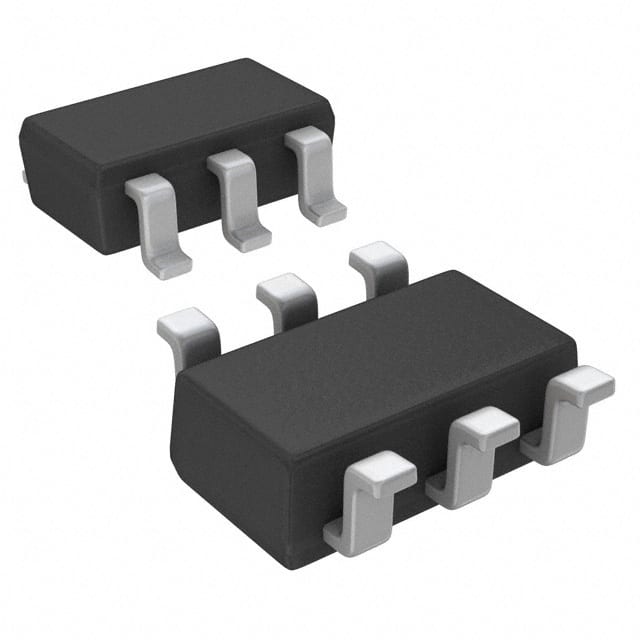
Package: The NLAST4599DTT1G is available in a small SOT-363 package, which is suitable for space-constrained applications.
Essence: The essence of the NLAST4599DTT1G lies in its ability to seamlessly translate signals between different voltage levels, enabling smooth communication between components operating at different voltages.
Packaging/Quantity: The NLAST4599DTT1G is typically sold in reels containing 3000 units per reel.
Specifications
- Supply Voltage Range: 1.2V to 3.6V
- Input Voltage Range (A Port): 0V to VCCA
- Input Voltage Range (B Port): 0V to VCCB
- Output Voltage Range (A Port): 0V to VCCA
- Output Voltage Range (B Port): 0V to VCCB
- Maximum Data Rate: 100 Mbps
- Operating Temperature Range: -40°C to +85°C
Detailed Pin Configuration
The NLAST4599DTT1G features a total of six pins:
- A1: Input/Output pin for Port A
- A2: Input/Output pin for Port A
- GND: Ground reference
- B2: Input/Output pin for Port B
- B1: Input/Output pin for Port B
- VCCA/VCCB: Supply voltage pins for Port A and Port B, respectively
Functional Features
- Bidirectional voltage translation between Port A and Port B
- Automatic direction control based on the input signal levels
- High-speed operation allows for seamless signal transmission
- Low power consumption ensures energy efficiency
- Wide voltage translation range accommodates various voltage levels
Advantages and Disadvantages
Advantages: - Enables communication between components operating at different voltage levels - Compact package size suitable for space-constrained applications - High-speed operation for efficient signal transmission - Low power consumption for energy efficiency
Disadvantages: - Limited to dual supply voltage translation - Maximum data rate may not be sufficient for certain high-speed applications
Working Principles
The NLAST4599DTT1G utilizes a combination of MOSFETs and level-shifting circuitry to achieve bidirectional voltage translation. The direction of translation is automatically controlled based on the input signal levels, ensuring seamless communication between different voltage domains.
Detailed Application Field Plans
The NLAST4599DTT1G finds applications in various electronic systems where voltage translation is required. Some potential application fields include: - Battery-powered devices - Mobile phones and tablets - Industrial automation systems - Consumer electronics - Automotive electronics
Detailed and Complete Alternative Models
- SN74LVC2T45: Dual-Bit Dual-Supply Bus Transceiver
- TXS0102: 2-Bit Bidirectional Voltage-Level Translator
- PCA9306: Dual Bidirectional I2C-Bus and SMBus Voltage-Level Translator
These alternative models offer similar functionality and can be considered as alternatives to the NLAST4599DTT1G based on specific application requirements.
Word count: 450 words
Noem 10 veelgestelde vragen en antwoorden met betrekking tot de toepassing van NLAST4599DTT1G in technische oplossingen
Sure! Here are 10 common questions and answers related to the application of NLAST4599DTT1G in technical solutions:
Q1: What is NLAST4599DTT1G? A1: NLAST4599DTT1G is a specific type of transistor, commonly known as a dual N-channel enhancement mode MOSFET.
Q2: What are the key features of NLAST4599DTT1G? A2: Some key features of NLAST4599DTT1G include low on-resistance, high current handling capability, and fast switching speed.
Q3: What are the typical applications of NLAST4599DTT1G? A3: NLAST4599DTT1G is often used in various technical solutions such as power management, motor control, and general-purpose switching applications.
Q4: What is the maximum voltage rating for NLAST4599DTT1G? A4: The maximum voltage rating for NLAST4599DTT1G is typically around 30 volts.
Q5: What is the maximum current rating for NLAST4599DTT1G? A5: The maximum continuous drain current rating for NLAST4599DTT1G is usually around 1.5 amps.
Q6: Can NLAST4599DTT1G be used for high-frequency applications? A6: NLAST4599DTT1G is not specifically designed for high-frequency applications, but it can still be used in moderate frequency switching applications.
Q7: Is NLAST4599DTT1G suitable for both analog and digital circuits? A7: Yes, NLAST4599DTT1G can be used in both analog and digital circuits due to its low on-resistance and fast switching characteristics.
Q8: Does NLAST4599DTT1G require any external components for operation? A8: NLAST4599DTT1G can be used as a standalone component, but it may require additional components such as resistors or capacitors depending on the specific application.
Q9: Can NLAST4599DTT1G handle high-temperature environments? A9: NLAST4599DTT1G has a maximum junction temperature rating of around 150 degrees Celsius, making it suitable for many high-temperature applications.
Q10: Is NLAST4599DTT1G readily available in the market? A10: Yes, NLAST4599DTT1G is a commonly available transistor and can be easily sourced from various electronic component suppliers.
Please note that the answers provided here are general and may vary based on specific datasheets and manufacturer specifications.