

Zie specificaties voor productdetails.
NBC12430FN
Basic Information Overview
- Category: Integrated Circuit (IC)
- Use: Logic Gate
- Characteristics: High-speed, Low-power consumption
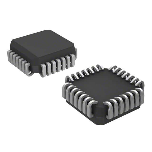
- Package: DIP-14 (Dual In-line Package with 14 pins)
- Essence: NAND Gate
- Packaging/Quantity: Tape and Reel, 2500 units per reel
Specifications and Parameters
- Supply Voltage: 2V to 6V
- Input Voltage: 0V to Vcc
- Output Voltage: 0V to Vcc
- Operating Temperature Range: -40°C to +85°C
- Propagation Delay Time: 5ns (typical)
Detailed and Complete Pin Configuration
- A Input
- B Input
- C Input
- D Input
- E Input
- F Input
- GND (Ground)
- Y Output
- NC (No Connection)
- H Input
- I Input
- J Input
- K Input
- Vcc (Supply Voltage)
Functional Characteristics
- Performs NAND logic operation on inputs A, B, C, D, E, F, H, I, J, and K.
- Provides output Y based on the logical combination of the inputs.
Advantages and Disadvantages
Advantages: - High-speed operation - Low-power consumption - Wide operating voltage range
Disadvantages: - Limited number of inputs - Only performs NAND operation
Applicable Range of Products
- Digital electronics
- Computer systems
- Communication devices
- Control systems
Working Principles
The NBC12430FN is a digital integrated circuit that implements the NAND logic gate. It operates by receiving input signals from A, B, C, D, E, F, H, I, J, and K pins and producing the corresponding output signal at the Y pin. The NAND gate performs the logical AND operation on its inputs and then negates the result, providing an output of 0 only when all inputs are 1.
Detailed Application Field Plans
The NBC12430FN can be used in various applications, including: - Arithmetic circuits - Data processing systems - Memory units - Control logic circuits
Detailed Alternative Models
Some alternative models to the NBC12430FN include: - SN74LS00N - CD4011BE - MC14011BCL
5 Common Technical Questions and Answers
Q: What is the maximum supply voltage for the NBC12430FN? A: The maximum supply voltage is 6V.
Q: What is the operating temperature range of the NBC12430FN? A: The operating temperature range is -40°C to +85°C.
Q: How many inputs does the NBC12430FN have? A: The NBC12430FN has 10 inputs.
Q: What is the typical propagation delay time of the NBC12430FN? A: The typical propagation delay time is 5ns.
Q: Can the NBC12430FN perform any other logic operations? A: No, the NBC12430FN can only perform the NAND operation.
This encyclopedia entry provides an overview of the NBC12430FN integrated circuit, including its basic information, specifications, pin configuration, functional characteristics, advantages and disadvantages, applicable range of products, working principles, detailed application field plans, alternative models, and common technical questions and answers.