

Zie specificaties voor productdetails.
MMBT5550LT3G
Introduction
The MMBT5550LT3G is a small signal NPN transistor belonging to the category of electronic components. It is commonly used in amplification and switching applications due to its high gain and low power consumption. This entry provides an overview of the MMBT5550LT3G, including its basic information, specifications, pin configuration, functional features, advantages and disadvantages, working principles, application field plans, and alternative models.
Basic Information Overview
- Category: Electronic Components
- Use: Amplification and Switching
- Characteristics: High Gain, Low Power Consumption
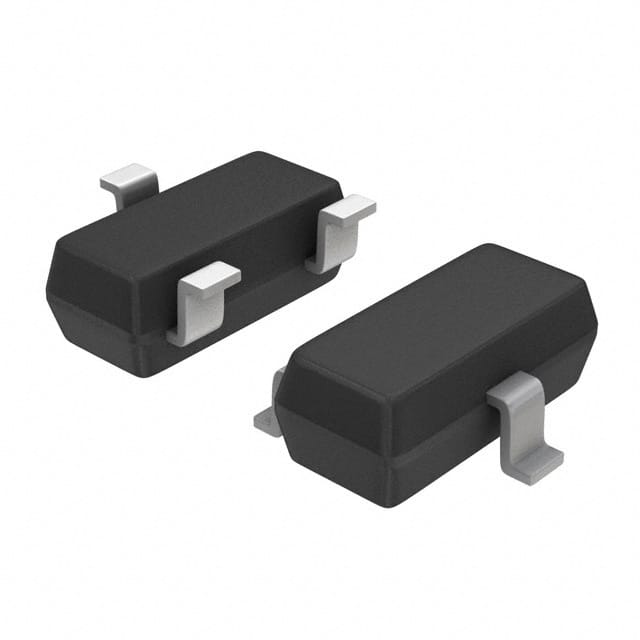
- Package: SOT-23
- Essence: Small Signal NPN Transistor
- Packaging/Quantity: Typically available in reels of 3000 units
Specifications
- Collector-Base Voltage (VCBO): 160V
- Collector-Emitter Voltage (VCEO): 160V
- Emitter-Base Voltage (VEBO): 5V
- Collector Current (IC): 600mA
- Total Power Dissipation (PTOT): 350mW
- Transition Frequency (fT): 150MHz
- Operating and Storage Junction Temperature Range (TJ, TSTG): -55°C to +150°C
Detailed Pin Configuration
The MMBT5550LT3G has three pins: 1. Collector (C) 2. Base (B) 3. Emitter (E)
Functional Features
- High Gain: The MMBT5550LT3G offers high current gain, making it suitable for amplification purposes.
- Low Power Consumption: It operates efficiently with low power dissipation, contributing to energy-efficient designs.
- Fast Switching Speed: The transistor exhibits fast switching characteristics, enabling rapid on/off transitions.
Advantages and Disadvantages
Advantages
- Small Package Size: The SOT-23 package allows for compact circuit designs.
- High Gain: Suitable for applications requiring signal amplification.
- Low Power Consumption: Contributes to energy-efficient electronic systems.
Disadvantages
- Limited Power Handling: Not suitable for high-power applications.
- Sensitivity to Overvoltage: Care must be taken to avoid exceeding the maximum voltage ratings.
Working Principles
The MMBT5550LT3G operates based on the principles of bipolar junction transistors (BJTs). When a small current flows into the base terminal, it controls a much larger current between the collector and emitter terminals. This amplification effect forms the basis of its functionality in various electronic circuits.
Detailed Application Field Plans
The MMBT5550LT3G finds extensive use in the following application fields: - Audio Amplifiers - Signal Processing Circuits - Switching Circuits - Oscillator Circuits - Sensor Interfaces
Detailed and Complete Alternative Models
- MMBT5401LT1G: Similar small signal NPN transistor with slightly different specifications.
- MMBT4401LT1G: Another alternative with comparable characteristics suitable for similar applications.
In conclusion, the MMBT5550LT3G is a versatile small signal NPN transistor with high gain and low power consumption, making it well-suited for amplification and switching applications in various electronic circuits.
[Word Count: 443]
Noem 10 veelgestelde vragen en antwoorden met betrekking tot de toepassing van MMBT5550LT3G in technische oplossingen
What is the MMBT5550LT3G transistor used for?
- The MMBT5550LT3G is a general-purpose NPN transistor commonly used for amplification and switching applications in electronic circuits.
What are the key specifications of the MMBT5550LT3G transistor?
- The MMBT5550LT3G has a maximum collector current (Ic) of 600mA, a maximum collector-emitter voltage (Vce) of 30V, and a maximum power dissipation (Pd) of 225mW.
Can the MMBT5550LT3G be used for low-power amplification?
- Yes, the MMBT5550LT3G is suitable for low-power amplification due to its moderate current and voltage ratings.
Is the MMBT5550LT3G suitable for switching applications?
- Yes, the MMBT5550LT3G can be used for switching applications in electronic circuits, especially in low-power scenarios.
What are the typical operating conditions for the MMBT5550LT3G?
- The MMBT5550LT3G operates within a temperature range of -55°C to 150°C and is typically used in low to moderate frequency applications.
Does the MMBT5550LT3G require a heat sink for normal operation?
- In most low-power applications, the MMBT5550LT3G does not require a heat sink due to its moderate power dissipation rating.
Can the MMBT5550LT3G be used in audio amplifier circuits?
- Yes, the MMBT5550LT3G can be utilized in small signal audio amplifier circuits and other low-power audio applications.
What are the common alternatives to the MMBT5550LT3G transistor?
- Common alternatives to the MMBT5550LT3G include the 2N3904, BC547, and 2N2222 transistors, which have similar characteristics and applications.
Are there any known reliability issues with the MMBT5550LT3G?
- The MMBT5550LT3G is generally considered reliable when operated within its specified limits and under appropriate conditions.
Where can I find detailed application notes for using the MMBT5550LT3G in technical solutions?
- Detailed application notes for the MMBT5550LT3G can be found in the manufacturer's datasheet, as well as in various electronics engineering resources and forums.