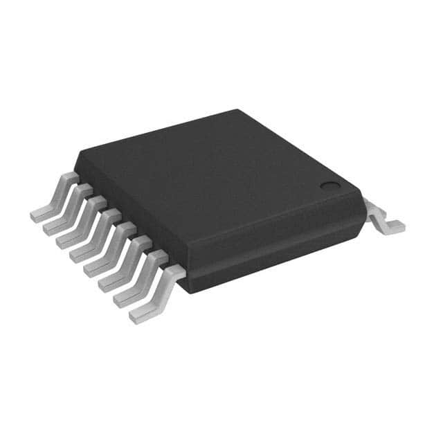
Zie specificaties voor productdetails.

MM74HC259MTCX
Product Overview
- Category: Integrated Circuit
- Use: Data Selector/Multiplexer
- Characteristics: High-Speed, CMOS Logic, 8-Bit, Addressable Latch/Buffer
- Package: TSSOP-16
- Essence: The MM74HC259MTCX is a versatile integrated circuit that can be used as a data selector or multiplexer. It features high-speed operation and is based on CMOS logic technology. The device has 8-bit addressable latch/buffer functionality.
- Packaging/Quantity: The MM74HC259MTCX is available in a TSSOP-16 package and is typically sold in reels of 2500 units.
Specifications
- Supply Voltage: 2V to 6V
- Operating Temperature Range: -40°C to +85°C
- Input Voltage Levels: High: 2V to Vcc, Low: GND to 0.8Vcc
- Output Voltage Levels: High: Vcc - 0.5V, Low: 0.5V
- Propagation Delay: 14ns (typical)
- Quiescent Current: 4μA (maximum)
Pin Configuration
The MM74HC259MTCX has a total of 16 pins arranged as follows:
__    __
   A7 |1  \__/ 16| Vcc
   A6 |2        15| Q0
   A5 |3        14| Q1
   A4 |4        13| Q2
   A3 |5        12| Q3
   A2 |6        11| Q4
   A1 |7        10| Q5
   A0 |8         9| Q6
  GND |__________|
Functional Features
- Addressable latch/buffer functionality allows individual control of each output pin.
- High-speed operation enables efficient data selection and multiplexing.
- CMOS logic technology ensures low power consumption and compatibility with a wide range of digital systems.
- Wide supply voltage range (2V to 6V) provides flexibility in various applications.
Advantages and Disadvantages
Advantages: - Versatile functionality as a data selector or multiplexer. - High-speed operation for efficient data handling. - Low power consumption due to CMOS technology. - Wide supply voltage range allows compatibility with different systems.
Disadvantages: - Limited number of addressable outputs (8 bits). - May require additional external components for certain applications.
Working Principles
The MM74HC259MTCX is designed to select and multiplex data based on the input address. The device has eight address inputs (A0-A7) that determine which output pin (Q0-Q6) is active. The latch/buffer functionality allows individual control of each output pin, providing flexibility in data routing.
When an address is applied to the address inputs, the corresponding output pin becomes active, reflecting the data present at the input. The selected output remains latched until a new address is applied. This latch/buffer behavior enables the MM74HC259MTCX to store and route data efficiently.
Detailed Application Field Plans
The MM74HC259MTCX can be used in various applications, including:
- Data Multiplexing: The device can be employed to select and route multiple data sources to a single destination, such as in communication systems or audio/video equipment.
- Address Decoding: It can be utilized to decode specific addresses and enable corresponding functions or devices in microcontroller-based systems.
- Memory Expansion: The MM74HC259MTCX can be used to expand the addressable memory space in systems with limited address lines.
- Control Signal Routing: It can be employed to route control signals based on specific conditions or events, enabling flexible system control.
Detailed and Complete Alternative Models
- CD74HC259E: Similar functionality and characteristics, available in a DIP-16 package.
- SN74HC259N: Equivalent device from a different manufacturer, available in a DIP-16 package.
- 74HCT259: Compatible device with TTL logic levels, available in various packages.
These alternative models provide similar functionality to the MM74HC259MTCX and can be considered as replacements depending on specific requirements and availability.
Word count: 534 words
Noem 10 veelgestelde vragen en antwoorden met betrekking tot de toepassing van MM74HC259MTCX in technische oplossingen
Sure! Here are 10 common questions and answers related to the application of MM74HC259MTCX in technical solutions:
Q: What is MM74HC259MTCX? A: MM74HC259MTCX is a 8-bit addressable latch with 3-state outputs, commonly used in digital circuits.
Q: What is the purpose of MM74HC259MTCX? A: The purpose of MM74HC259MTCX is to store and control data in digital systems, allowing for efficient addressing and manipulation of multiple inputs and outputs.
Q: How does MM74HC259MTCX work? A: MM74HC259MTCX has an 8-bit input register that stores data, which can be latched onto its outputs using an enable signal. It also has 3-state outputs that can be enabled or disabled.
Q: What voltage levels does MM74HC259MTCX support? A: MM74HC259MTCX supports a wide range of voltage levels, typically between 2V and 6V.
Q: Can MM74HC259MTCX be cascaded to increase the number of addressable outputs? A: Yes, MM74HC259MTCX can be cascaded by connecting the output of one latch to the input of another, allowing for expansion of the number of addressable outputs.
Q: What is the maximum frequency at which MM74HC259MTCX can operate? A: MM74HC259MTCX can operate at frequencies up to several hundred megahertz (MHz), depending on the specific conditions and setup.
Q: Is MM74HC259MTCX compatible with TTL logic levels? A: Yes, MM74HC259MTCX is compatible with TTL logic levels, making it suitable for interfacing with a wide range of digital systems.
Q: Can MM74HC259MTCX be used in both synchronous and asynchronous applications? A: Yes, MM74HC259MTCX can be used in both synchronous and asynchronous applications, depending on the specific requirements of the system.
Q: What are the typical applications of MM74HC259MTCX? A: MM74HC259MTCX is commonly used in address decoding, data multiplexing, LED matrix control, memory expansion, and other digital systems requiring efficient data storage and manipulation.
Q: Where can I find more information about MM74HC259MTCX? A: You can refer to the datasheet provided by the manufacturer or visit their official website for detailed information about MM74HC259MTCX, including its specifications, pinout, and application examples.
Please note that the answers provided here are general and may vary depending on the specific implementation and requirements of your technical solution.

