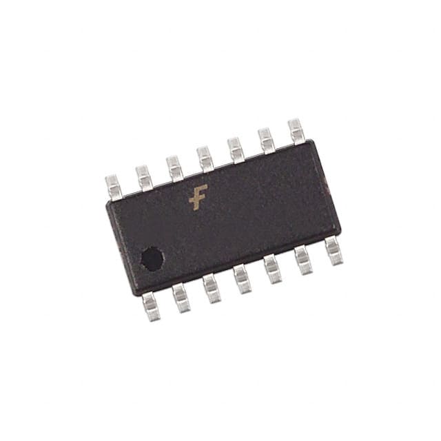
Zie specificaties voor productdetails.

Encyclopedia Entry: 74F74SJX
Product Overview
Category
The 74F74SJX belongs to the category of integrated circuits (ICs), specifically flip-flop ICs.
Use
This IC is commonly used in digital electronics for storing and manipulating binary data. It serves as a fundamental building block in various applications, including sequential logic circuits, counters, registers, and memory units.
Characteristics
- The 74F74SJX operates on a supply voltage range of 4.5V to 5.5V.
- It features two independent D-type positive-edge-triggered flip-flops with complementary outputs.
- The IC is designed to provide high-speed performance and low power consumption.
- It offers excellent noise immunity and robustness against electrical disturbances.
Package and Quantity
The 74F74SJX is typically available in a small outline integrated circuit (SOIC) package. Each package contains one IC.
Specifications
- Supply Voltage Range: 4.5V to 5.5V
- Logic Family: 74F
- Flip-Flop Type: D-Type Positive-Edge-Triggered
- Number of Flip-Flops: 2
- Output Type: Complementary
- Operating Temperature Range: -40°C to +85°C
Pin Configuration
The detailed pin configuration of the 74F74SJX is as follows:
+---+--+---+
   Q1 |1     14| VCC
   D1 |2     13| Q2
  CLK |3     12| CLR
   PR |4     11| D2
   PL |5     10| GND
   Q1 |6      9| D2
   D1 |7      8| CLK
       +--------+
Functional Features
- Positive-edge-triggered operation: The flip-flops store the input data (D1 and D2) at the rising edge of the clock signal (CLK).
- Complementary outputs: Each flip-flop provides both Q and Q̅ outputs, ensuring the availability of inverted signals.
- Clear and preset inputs: The CLR and PR pins allow for asynchronous clearing and presetting of the flip-flops.
- High-speed performance: The 74F74SJX is designed to operate at high clock frequencies, making it suitable for time-critical applications.
Advantages and Disadvantages
Advantages: - High-speed operation enables efficient processing of digital signals. - Low power consumption contributes to energy-efficient designs. - Excellent noise immunity ensures reliable operation in noisy environments.
Disadvantages: - Limited voltage supply range restricts compatibility with certain systems. - Small package size may require careful handling during assembly.
Working Principles
The 74F74SJX operates based on the principles of sequential logic. The flip-flops within the IC store binary data using feedback loops. The stored data can be manipulated by applying appropriate clock signals and control inputs. This allows for the creation of complex digital circuits that perform various functions, such as counting, storing, and transferring data.
Application Field Plans
The 74F74SJX finds extensive use in numerous digital electronic applications, including: - Microprocessor-based systems - Data storage and retrieval systems - Communication equipment - Industrial automation systems - Consumer electronics
Alternative Models
For similar functionality, alternative models to the 74F74SJX include: - 74LS74 - 74HC74 - 74HCT74 - CD4013 - SN74LVC2G74
These alternative models offer comparable features and can be used as substitutes depending on specific design requirements.
In conclusion, the 74F74SJX is a versatile flip-flop IC that provides high-speed performance, low power consumption, and excellent noise immunity. Its application spans across various digital electronic systems, making it an essential component in modern technology.
Word Count: 450
Noem 10 veelgestelde vragen en antwoorden met betrekking tot de toepassing van 74F74SJX in technische oplossingen
Sure! Here are 10 common questions and answers related to the application of 74F74SJX in technical solutions:
Q: What is the 74F74SJX? A: The 74F74SJX is a dual D-type flip-flop integrated circuit (IC) that can store one bit of data.
Q: What is the purpose of using the 74F74SJX in technical solutions? A: The 74F74SJX is commonly used for sequential logic applications, such as storing and transferring data in digital systems.
Q: How many flip-flops are there in the 74F74SJX IC? A: The 74F74SJX contains two independent D-type flip-flops.
Q: What is the maximum clock frequency supported by the 74F74SJX? A: The 74F74SJX typically supports clock frequencies up to several hundred megahertz (MHz).
Q: Can the 74F74SJX be used for edge-triggered or level-triggered operations? A: Yes, the 74F74SJX can be configured for both edge-triggered and level-triggered operations based on the input connections.
Q: What is the power supply voltage range for the 74F74SJX? A: The 74F74SJX typically operates with a power supply voltage range of 4.5V to 5.5V.
Q: Does the 74F74SJX have any built-in protection features? A: Yes, the 74F74SJX includes built-in protection against electrostatic discharge (ESD) and excessive power supply voltage.
Q: Can the 74F74SJX be cascaded to create larger storage capacities? A: Yes, multiple 74F74SJX ICs can be cascaded together to create larger storage capacities by connecting the outputs of one flip-flop to the inputs of another.
Q: What are the typical applications of the 74F74SJX? A: The 74F74SJX is commonly used in digital systems for tasks such as data synchronization, frequency division, and state machine design.
Q: Are there any specific timing considerations when using the 74F74SJX? A: Yes, the 74F74SJX has specific setup and hold time requirements that need to be met to ensure proper operation. These timings are mentioned in the datasheet and should be carefully considered during circuit design.
Please note that the answers provided here are general and may vary depending on the specific implementation and requirements of your technical solution. It's always recommended to refer to the datasheet and consult with an expert for accurate and detailed information.

