

Zie specificaties voor productdetails.
N74F269DB,118
Basic Information Overview
- Category: Integrated Circuit (IC)
- Use: Digital Logic Device
- Characteristics:
- High-speed operation
- Low power consumption
- Wide operating voltage range
- Compact package size
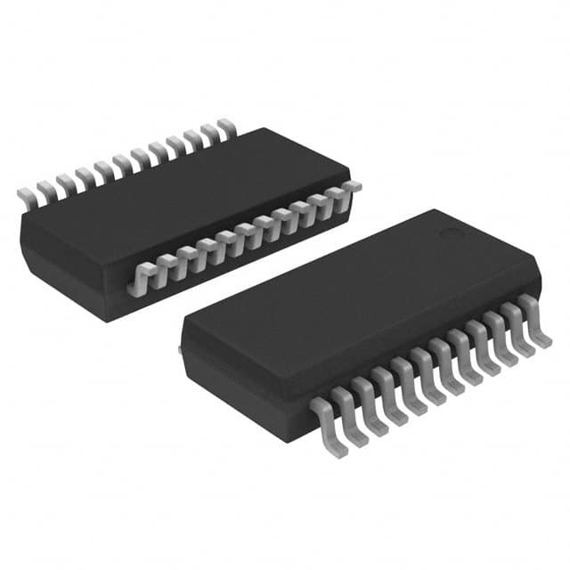
- Package: SOIC (Small Outline Integrated Circuit)
- Essence: Flip-Flop with Clear and Preset
- Packaging/Quantity: Tape and Reel, 2500 units per reel
Specifications
- Supply Voltage Range: 2V to 6V
- Input Voltage Range: 0V to VCC
- Operating Temperature Range: -40°C to +85°C
- Output Current: ±6mA
- Propagation Delay Time: 10ns (max)
- Power Dissipation: 500mW (max)
Detailed Pin Configuration
The N74F269DB,118 IC has a total of 16 pins. The pin configuration is as follows:
| Pin No. | Name | Description | |---------|------|-------------| | 1 | CP | Clock Pulse Input | | 2 | D | Data Input | | 3 | P | Preset Input | | 4 | C | Clear Input | | 5 | Q0 | Output Q0 | | 6 | Q1 | Output Q1 | | 7 | Q2 | Output Q2 | | 8 | GND | Ground | | 9 | Q3 | Output Q3 | | 10 | Q4 | Output Q4 | | 11 | Q5 | Output Q5 | | 12 | Q6 | Output Q6 | | 13 | Q7 | Output Q7 | | 14 | VCC | Supply Voltage | | 15 | MR | Master Reset Input | | 16 | OE | Output Enable Input |
Functional Features
- The N74F269DB,118 is a flip-flop IC with clear and preset functionality.
- It operates at high speed and consumes low power.
- The wide operating voltage range makes it suitable for various applications.
- The compact package size allows for space-efficient designs.
Advantages and Disadvantages
Advantages: - High-speed operation enables quick data processing. - Low power consumption helps in energy-efficient designs. - Wide operating voltage range provides flexibility in different power supply scenarios. - Compact package size saves board space and allows for miniaturization.
Disadvantages: - Limited output current may restrict certain applications requiring higher current. - Propagation delay time may affect real-time applications with strict timing requirements.
Working Principles
The N74F269DB,118 is a synchronous, edge-triggered flip-flop. It stores and transfers data based on the clock pulse input (CP). The data input (D) determines the state of the flip-flop, while the preset (P) and clear (C) inputs allow for specific initialization conditions. The outputs (Q0-Q7) represent the stored data. The master reset (MR) input resets the flip-flop to a known state, and the output enable (OE) input controls the output stage.
Detailed Application Field Plans
The N74F269DB,118 IC finds applications in various digital systems, including but not limited to: - Microprocessors and microcontrollers - Communication systems - Data storage devices - Industrial automation - Consumer electronics
Detailed and Complete Alternative Models
Some alternative models that offer similar functionality to the N74F269DB,118 IC are: - SN74LS273 - CD4013BE - MC74HC73AN - 74HCT574
These alternative models can be considered based on specific requirements and availability.
Word count: 413 words
Noem 10 veelgestelde vragen en antwoorden met betrekking tot de toepassing van N74F269DB,118 in technische oplossingen
Sure! Here are 10 common questions and answers related to the application of N74F269DB,118 in technical solutions:
Q: What is the N74F269DB,118? A: The N74F269DB,118 is a specific type of integrated circuit (IC) or chip that belongs to the NXP Semiconductors family. It is a 8-bit binary counter with asynchronous reset.
Q: What is the purpose of the N74F269DB,118? A: The N74F269DB,118 is commonly used as a counter in various digital applications, such as frequency dividers, event counters, and general-purpose counting circuits.
Q: How many bits does the N74F269DB,118 have? A: The N74F269DB,118 is an 8-bit counter, meaning it can count up to 256 different states before resetting.
Q: Does the N74F269DB,118 require an external clock signal? A: Yes, the N74F269DB,118 requires an external clock signal to increment its count. The clock input is labeled as "CLK" on the chip.
Q: Can the N74F269DB,118 be cascaded to create larger counters? A: Yes, multiple N74F269DB,118 chips can be cascaded together to create larger counters with more bits.
Q: What is the power supply voltage range for the N74F269DB,118? A: The N74F269DB,118 operates within a power supply voltage range of 4.5V to 5.5V.
Q: Does the N74F269DB,118 have any special features or additional inputs/outputs? A: The N74F269DB,118 has an asynchronous reset input (labeled as "RST") that allows you to reset the counter to a specific state.
Q: What is the maximum clock frequency that the N74F269DB,118 can handle? A: The N74F269DB,118 can typically handle clock frequencies up to 100 MHz, but it's always recommended to refer to the datasheet for precise specifications.
Q: Can the N74F269DB,118 be used in both digital and analog applications? A: No, the N74F269DB,118 is specifically designed for digital applications and is not suitable for analog circuits.
Q: Are there any specific precautions or considerations when using the N74F269DB,118? A: It is important to ensure proper decoupling capacitors are used near the power supply pins of the chip to minimize noise and voltage fluctuations. Additionally, following the recommended operating conditions and timing diagrams provided in the datasheet is crucial for reliable operation.
Please note that these answers are general and may vary depending on the specific application and requirements. Always refer to the datasheet and consult with technical experts for accurate information.