

Zie specificaties voor productdetails.
Encyclopedia Entry: 74ALVT16601DL,518
Product Overview
Category
The 74ALVT16601DL,518 belongs to the category of integrated circuits (ICs).
Use
This IC is commonly used in digital electronic systems for data processing and signal transmission.
Characteristics
- High-speed operation
- Low power consumption
- Wide operating voltage range
- Compatibility with various logic families
- Robustness against noise and interference
Package
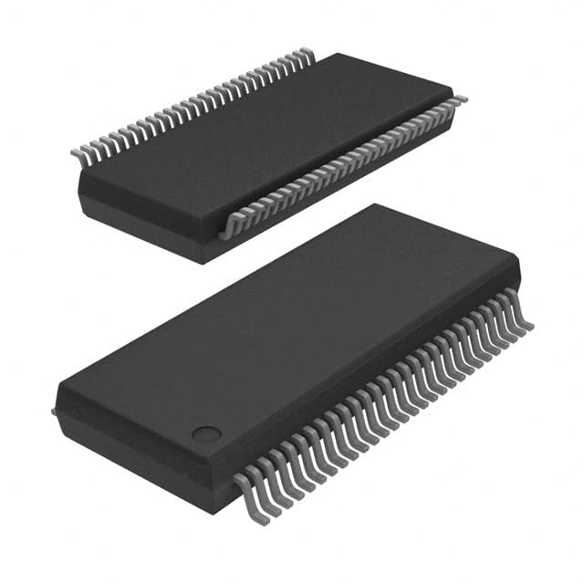
The 74ALVT16601DL,518 is available in a small outline package (SOP) or a thin shrink small outline package (TSSOP).
Essence
This IC serves as a versatile interface between different components of a digital system, enabling efficient data transfer and synchronization.
Packaging/Quantity
The 74ALVT16601DL,518 is typically packaged in reels or tubes, with quantities varying based on customer requirements.
Specifications
- Supply Voltage: 2.3V to 3.6V
- Input Voltage: 0V to VCC
- Output Voltage: 0V to VCC
- Operating Temperature Range: -40°C to +85°C
- Logic Family: ALVT
Detailed Pin Configuration
The 74ALVT16601DL,518 consists of 48 pins, each serving a specific function within the circuit. The pin configuration is as follows:
- Pin 1: Output Enable (OE)
- Pin 2: Data Input A0
- Pin 3: Data Input A1
- Pin 4: Data Input A2
- Pin 5: Data Input A3
- Pin 6: Data Input A4
- Pin 7: Data Input A5
- Pin 8: Data Input A6
- Pin 9: Data Input A7
- Pin 10: Data Input A8
- Pin 11: Data Input A9
- Pin 12: Data Input A10
- Pin 13: Data Input A11
- Pin 14: Data Input A12
- Pin 15: Data Input A13
- Pin 16: Data Input A14
- Pin 17: Data Input A15
- Pin 18: Output Y0
- Pin 19: Output Y1
- Pin 20: Output Y2
- Pin 21: Output Y3
- Pin 22: Output Y4
- Pin 23: Output Y5
- Pin 24: Output Y6
- Pin 25: Output Y7
- Pin 26: Output Y8
- Pin 27: Output Y9
- Pin 28: Output Y10
- Pin 29: Output Y11
- Pin 30: Output Y12
- Pin 31: Output Y13
- Pin 32: Output Y14
- Pin 33: Output Y15
- Pin 34: GND (Ground)
- Pin 35: VCC (Supply Voltage)
- Pin 36: Data Input B0
- Pin 37: Data Input B1
- Pin 38: Data Input B2
- Pin 39: Data Input B3
- Pin 40: Data Input B4
- Pin 41: Data Input B5
- Pin 42: Data Input B6
- Pin 43: Data Input B7
- Pin 44: Data Input B8
- Pin 45: Data Input B9
- Pin 46: Data Input B10
- Pin 47: Data Input B11
- Pin 48: Data Input B12
Functional Features
The 74ALVT16601DL,518 offers the following functional features:
- Bidirectional data transfer between two independent buses (A and B)
- Output enable control for tri-state outputs
- High-speed operation for efficient data processing
- Wide operating voltage range for compatibility with various systems
- Robustness against noise and interference for reliable signal transmission
Advantages and Disadvantages
Advantages
- High-speed operation allows for quick data transfer
- Low power consumption minimizes energy usage
- Compatibility with different logic families enhances versatility
- Wide operating voltage range enables integration into various systems
- Robustness against noise ensures reliable signal transmission
Disadvantages
- Limited number of input/output pins may restrict complex system designs
- Higher cost compared to some alternative models
Working Principles
The 74ALVT16601DL,518 operates based on the principles of digital logic. It utilizes a combination of transistors, resistors, and
Noem 10 veelgestelde vragen en antwoorden met betrekking tot de toepassing van 74ALVT16601DL,518 in technische oplossingen
Sure! Here are 10 common questions and answers related to the application of 74ALVT16601DL,518:
Q: What is the function of the 74ALVT16601DL,518? A: The 74ALVT16601DL,518 is a 18-bit universal bus driver with 3-state outputs.
Q: What is the operating voltage range for this device? A: The operating voltage range for the 74ALVT16601DL,518 is typically between 2.7V and 3.6V.
Q: How many 3-state outputs does this device have? A: The 74ALVT16601DL,518 has 18 3-state outputs.
Q: Can this device be used in both parallel and serial data transfer applications? A: Yes, the 74ALVT16601DL,518 can be used in both parallel and serial data transfer applications.
Q: What is the maximum frequency at which this device can operate? A: The maximum frequency at which the 74ALVT16601DL,518 can operate is typically around 200MHz.
Q: Does this device have any built-in protection features? A: Yes, the 74ALVT16601DL,518 has built-in ESD protection on all inputs and outputs.
Q: Can this device be used in automotive applications? A: Yes, the 74ALVT16601DL,518 is qualified for automotive applications according to the AEC-Q100 standard.
Q: What is the power supply current consumption of this device? A: The power supply current consumption of the 74ALVT16601DL,518 is typically around 20mA.
Q: Can this device be used in both CMOS and TTL logic systems? A: Yes, the 74ALVT16601DL,518 is compatible with both CMOS and TTL logic systems.
Q: What is the package type for this device? A: The 74ALVT16601DL,518 is available in a TSSOP (Thin Shrink Small Outline Package) package.
Please note that the answers provided here are general and may vary depending on the specific datasheet and manufacturer's specifications for the 74ALVT16601DL,518.