

Zie specificaties voor productdetails.
74ALVC374BQ,115
Product Overview
- Category: Integrated Circuit (IC)
- Use: Flip-Flop
- Characteristics: High-speed, low-power, non-inverting, edge-triggered D-type flip-flop
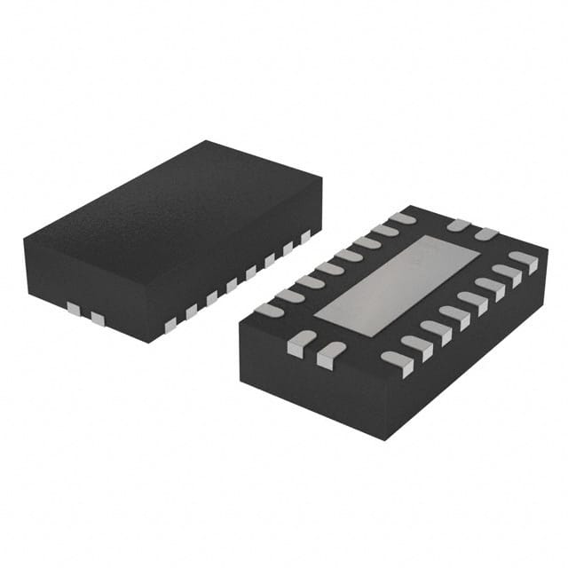
- Package: TSSOP (Thin Shrink Small Outline Package)
- Essence: This IC is designed to store and transfer data in digital systems.
- Packaging/Quantity: Available in reels of 2500 pieces
Specifications
- Supply Voltage Range: 1.2V to 3.6V
- Input Voltage Range: -0.5V to VCC + 0.5V
- Output Voltage Range: 0V to VCC
- Operating Temperature Range: -40°C to +85°C
- Propagation Delay Time: 2.8ns (typical)
- Output Drive Capability: ±24mA
Detailed Pin Configuration
The 74ALVC374BQ,115 IC has a total of 20 pins. The pin configuration is as follows:
- GND (Ground)
- D0 (Data Input 0)
- D1 (Data Input 1)
- D2 (Data Input 2)
- D3 (Data Input 3)
- D4 (Data Input 4)
- D5 (Data Input 5)
- D6 (Data Input 6)
- D7 (Data Input 7)
- OE (Output Enable)
- CP (Clock Pulse)
- MR (Master Reset)
- Q0 (Flip-Flop Output 0)
- Q1 (Flip-Flop Output 1)
- Q2 (Flip-Flop Output 2)
- Q3 (Flip-Flop Output 3)
- Q4 (Flip-Flop Output 4)
- Q5 (Flip-Flop Output 5)
- Q6 (Flip-Flop Output 6)
- VCC (Supply Voltage)
Functional Features
- Non-inverting D-type flip-flop with 3-state outputs
- Edge-triggered clock input for synchronous operation
- Master reset input to clear all flip-flops simultaneously
- Output enable input to put the outputs in high-impedance state
- High-speed operation suitable for high-frequency applications
- Low-power consumption for energy-efficient designs
Advantages and Disadvantages
Advantages: - High-speed operation allows for efficient data transfer - Low-power consumption helps in reducing overall system power requirements - 3-state outputs provide flexibility in connecting multiple devices - Edge-triggered clock input ensures synchronized data storage
Disadvantages: - Limited output drive capability may not be suitable for driving heavy loads - Requires external components for proper functioning in a digital system - Sensitive to voltage fluctuations, requiring stable power supply conditions
Working Principles
The 74ALVC374BQ,115 is a positive-edge-triggered D-type flip-flop. It stores and transfers data based on the rising edge of the clock signal. When the clock input (CP) transitions from low to high, the data present at the D0-D7 inputs is latched and stored in the corresponding flip-flop outputs (Q0-Q6). The output enable (OE) input controls whether the outputs are active or in a high-impedance state. The master reset (MR) input clears all flip-flops simultaneously when activated.
Detailed Application Field Plans
The 74ALVC374BQ,115 IC finds applications in various digital systems where data storage and transfer are required. Some potential application fields include:
- Microcontrollers: Used for storing and transferring data between different peripherals and memory units.
- Communication Systems: Enables data buffering and synchronization in high-speed data transmission.
- Data Processing Units: Facilitates data storage and manipulation in arithmetic and logic operations.
- Industrial Automation: Helps in controlling and monitoring processes by storing and transferring sensor data.
- Consumer Electronics: Used in devices like smartphones, tablets, and gaming consoles for data handling.
Detailed and Complete Alternative Models
- 74HC374: Similar flip-flop IC with comparable specifications but operates at a higher voltage range (2V to 6V).
- SN74LV374A: Low-voltage version of the flip-flop IC with similar characteristics and pin configuration.
- CD4013B: Dual D-type flip-flop IC with complementary outputs and wider operating temperature range (-55°C to +125°C).
(Note: The above alternative models are provided as examples and not an exhaustive list.)
This concludes the encyclopedia entry for the 74ALVC374BQ,115 IC, covering its product details, specifications, features, advantages, disadvantages, working principles, application fields, and alternative models.
Noem 10 veelgestelde vragen en antwoorden met betrekking tot de toepassing van 74ALVC374BQ,115 in technische oplossingen
Sure! Here are 10 common questions and answers related to the application of 74ALVC374BQ,115:
Question: What is the function of the 74ALVC374BQ,115?
Answer: The 74ALVC374BQ,115 is an octal D-type flip-flop with 3-state outputs.Question: What is the operating voltage range for this IC?
Answer: The operating voltage range for the 74ALVC374BQ,115 is 1.65V to 3.6V.Question: How many flip-flops are there in the 74ALVC374BQ,115?
Answer: There are 8 flip-flops in the 74ALVC374BQ,115.Question: What is the maximum clock frequency supported by this IC?
Answer: The maximum clock frequency supported by the 74ALVC374BQ,115 is 200MHz.Question: Can I use this IC in a 5V system?
Answer: No, the 74ALVC374BQ,115 is not compatible with 5V systems. It operates at lower voltages.Question: What is the output drive strength of this IC?
Answer: The output drive strength of the 74ALVC374BQ,115 is typically 24mA.Question: Does this IC have internal pull-up or pull-down resistors?
Answer: No, the 74ALVC374BQ,115 does not have internal pull-up or pull-down resistors.Question: Can I connect the outputs directly to other ICs?
Answer: Yes, the outputs of the 74ALVC374BQ,115 can be connected directly to other ICs.Question: What is the power supply current consumption of this IC?
Answer: The power supply current consumption of the 74ALVC374BQ,115 is typically 10μA.Question: Is this IC suitable for high-speed applications?
Answer: Yes, the 74ALVC374BQ,115 is designed for high-speed applications with its maximum clock frequency of 200MHz.
Please note that these answers are general and may vary depending on specific datasheet specifications and application requirements.