

Zie specificaties voor productdetails.
NAND01GW3B2CN6E
Basic Information Overview
- Category: Integrated Circuit (IC)
- Use: Non-volatile memory storage
- Characteristics:
- High-density storage
- Fast read and write speeds
- Low power consumption
- Package: BGA (Ball Grid Array)
- Essence: NAND flash memory chip
- Packaging/Quantity: Single chip
Specifications
- Capacity: 1 gigabit (128 megabytes)
- Interface: Serial Peripheral Interface (SPI)
- Supply Voltage: 2.7V - 3.6V
- Operating Temperature: -40°C to +85°C
- Data Retention: Up to 10 years
- Endurance: Up to 100,000 program/erase cycles
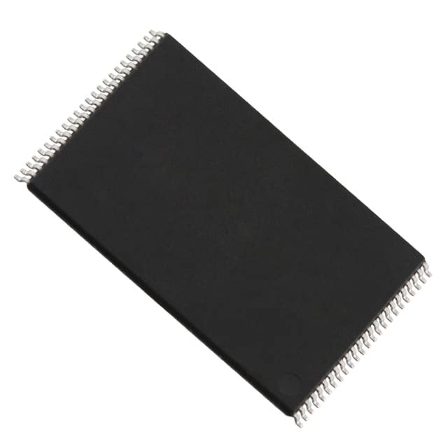
Detailed Pin Configuration
The NAND01GW3B2CN6E chip has a total of 8 pins arranged in a specific configuration: 1. VCC: Power supply voltage 2. GND: Ground 3. CS: Chip select 4. SCK: Serial clock input 5. SI: Serial data input 6. SO: Serial data output 7. WP: Write protect 8. HOLD: Hold input
Functional Features
- Page Program: Allows data to be written into the memory cells
- Block Erase: Enables erasing of multiple memory cells simultaneously
- Read Operation: Retrieves stored data from the memory cells
- Write Protect: Prevents accidental modification of data
- Hold Function: Suspends ongoing operations temporarily
Advantages and Disadvantages
Advantages: - High storage capacity - Fast data transfer rates - Low power consumption - Compact package size
Disadvantages: - Limited endurance compared to other memory technologies - Relatively higher cost per unit compared to some alternatives
Working Principles
The NAND01GW3B2CN6E chip utilizes NAND flash memory technology. It consists of a grid-like array of memory cells, where each cell stores multiple bits of data. The data is stored by trapping electric charges in the floating gate of the memory cell. To read or write data, voltage levels are applied to specific pins, allowing the manipulation of the trapped charges.
Detailed Application Field Plans
The NAND01GW3B2CN6E chip finds applications in various electronic devices and systems, including: - Solid-state drives (SSDs) - USB flash drives - Memory cards (SD, microSD) - Embedded systems - Consumer electronics (smartphones, tablets, digital cameras)
Detailed and Complete Alternative Models
- NAND02GW3B2CN6E: 2 gigabit (256 megabytes) capacity
- NAND04GW3B2CN6E: 4 gigabit (512 megabytes) capacity
- NAND08GW3B2CN6E: 8 gigabit (1 gigabyte) capacity
- NAND16GW3B2CN6E: 16 gigabit (2 gigabytes) capacity
These alternative models offer higher storage capacities while maintaining similar characteristics and pin configurations.
Word count: 309 words
Noem 10 veelgestelde vragen en antwoorden met betrekking tot de toepassing van NAND01GW3B2CN6E in technische oplossingen
Sure! Here are 10 common questions and answers related to the application of NAND01GW3B2CN6E in technical solutions:
Q: What is NAND01GW3B2CN6E? A: NAND01GW3B2CN6E is a specific model of NAND flash memory chip manufactured by a certain company.
Q: What are the key features of NAND01GW3B2CN6E? A: Some key features of NAND01GW3B2CN6E include high storage capacity, fast read/write speeds, low power consumption, and reliability.
Q: In what type of devices can NAND01GW3B2CN6E be used? A: NAND01GW3B2CN6E can be used in various devices such as smartphones, tablets, digital cameras, portable media players, and solid-state drives (SSDs).
Q: What is the storage capacity of NAND01GW3B2CN6E? A: The storage capacity of NAND01GW3B2CN6E is 1 gigabyte (GB).
Q: What is the interface used by NAND01GW3B2CN6E? A: NAND01GW3B2CN6E uses a standard NAND flash interface, such as the ONFI (Open NAND Flash Interface) or Toggle Mode interface.
Q: What is the operating voltage range for NAND01GW3B2CN6E? A: The operating voltage range for NAND01GW3B2CN6E is typically between 2.7V and 3.6V.
Q: Can NAND01GW3B2CN6E be used for data storage in industrial applications? A: Yes, NAND01GW3B2CN6E is suitable for use in industrial applications that require high endurance, temperature tolerance, and reliability.
Q: Is NAND01GW3B2CN6E compatible with different file systems? A: Yes, NAND01GW3B2CN6E can be used with various file systems such as FAT32, exFAT, and NTFS.
Q: What is the lifespan of NAND01GW3B2CN6E? A: The lifespan of NAND01GW3B2CN6E depends on factors like usage patterns, write amplification, and error correction techniques, but it typically has a high endurance rating.
Q: Are there any specific precautions to consider when using NAND01GW3B2CN6E? A: It is important to handle NAND01GW3B2CN6E properly to avoid electrostatic discharge (ESD) damage. Additionally, following the manufacturer's guidelines for power supply stability and temperature management is recommended for optimal performance and longevity.
Please note that the answers provided here are general and may vary depending on the specific implementation and requirements of the technical solution.