

Zie specificaties voor productdetails.
SY100S371JZ
Product Overview
- Category: Integrated Circuit (IC)
- Use: Logic Gate
- Characteristics: High-speed, low-power consumption
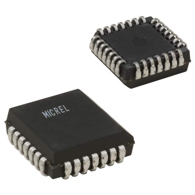
- Package: 20-pin plastic DIP (Dual In-line Package)
- Essence: Advanced logic gate with multiple functions
- Packaging/Quantity: Available in reels of 250 units
Specifications
- Supply Voltage: 4.5V to 5.5V
- Operating Temperature Range: -40°C to +85°C
- Input Voltage Range: 0V to VCC
- Output Voltage Range: 0V to VCC
- Propagation Delay Time: 1.5ns (typical)
- Power Dissipation: 500mW (max)
Detailed Pin Configuration
The SY100S371JZ has a total of 20 pins, which are assigned specific functions as follows:
- CLK (Clock Input)
- /CLK (Inverted Clock Input)
- GND (Ground)
- Q0 (Output 0)
- Q1 (Output 1)
- Q2 (Output 2)
- Q3 (Output 3)
- Q4 (Output 4)
- Q5 (Output 5)
- Q6 (Output 6)
- Q7 (Output 7)
- Q8 (Output 8)
- Q9 (Output 9)
- Q10 (Output 10)
- Q11 (Output 11)
- VCC (Supply Voltage)
- /OE (Output Enable)
- /CLR (Clear Input)
- /PRE (Preset Input)
- /LOAD (Load Input)
Functional Features
- The SY100S371JZ is a versatile logic gate that combines multiple functions into a single integrated circuit.
- It operates at high speeds and consumes low power, making it suitable for various applications.
- The device features 12 output pins (Q0 to Q11) that can be individually controlled.
- It supports clocked operations with the CLK and /CLK inputs.
- The /OE input allows for enabling or disabling the outputs.
- The /CLR and /PRE inputs provide additional control over the circuit's behavior.
- The /LOAD input enables loading of data into the circuit.
Advantages and Disadvantages
Advantages: - High-speed operation - Low power consumption - Compact size due to integration of multiple functions - Versatile functionality
Disadvantages: - Limited number of output pins - Requires external components for complete system implementation
Working Principles
The SY100S371JZ operates based on advanced logic gate principles. It utilizes clock signals to synchronize its internal operations and provides a range of output options. By controlling the inputs and utilizing the clock signal, users can achieve desired logic operations and manipulate the outputs accordingly.
Detailed Application Field Plans
The SY100S371JZ finds applications in various fields, including:
- Telecommunications: Used in high-speed data transmission systems.
- Networking: Employed in network switches and routers for efficient data processing.
- Industrial Automation: Integrated into control systems for precise timing and logic operations.
- Test and Measurement: Utilized in test equipment for accurate signal analysis.
- Consumer Electronics: Incorporated into devices requiring high-speed logic operations, such as gaming consoles and multimedia systems.
Detailed and Complete Alternative Models
- SY100S371JZ-TR: Tape and reel packaging option for automated assembly.
- SY100S371JZ-E3: Extended temperature range version (-55°C to +125°C).
- SY100S371JZ-Q1: Automotive-grade variant for use in automotive applications.
- SY100S371JZ-SP: Solder paste compatible packaging for surface mount assembly.
These alternative models offer similar functionality to the SY100S371JZ, but with specific variations to cater to different requirements and environments.
Word count: 495 words
Noem 10 veelgestelde vragen en antwoorden met betrekking tot de toepassing van SY100S371JZ in technische oplossingen
Sure! Here are 10 common questions and answers related to the application of SY100S371JZ in technical solutions:
Q: What is SY100S371JZ? A: SY100S371JZ is a specific integrated circuit (IC) chip used in various technical solutions.
Q: What are the main features of SY100S371JZ? A: SY100S371JZ is known for its high-speed operation, low power consumption, and compatibility with different logic families.
Q: In what applications can SY100S371JZ be used? A: SY100S371JZ can be used in applications such as clock distribution, data synchronization, and signal buffering.
Q: What is the operating voltage range of SY100S371JZ? A: The operating voltage range of SY100S371JZ typically falls between 4.5V and 5.5V.
Q: Can SY100S371JZ handle multiple input signals? A: Yes, SY100S371JZ has multiple input channels that can handle simultaneous signals.
Q: Does SY100S371JZ support bidirectional communication? A: No, SY100S371JZ is a unidirectional IC and does not support bidirectional communication.
Q: What is the maximum frequency that SY100S371JZ can handle? A: SY100S371JZ can handle frequencies up to several hundred megahertz (MHz).
Q: Is SY100S371JZ compatible with other logic families? A: Yes, SY100S371JZ is compatible with various logic families such as TTL, CMOS, and ECL.
Q: Can SY100S371JZ be used in high-temperature environments? A: Yes, SY100S371JZ is designed to operate reliably in high-temperature environments.
Q: Are there any specific precautions to consider when using SY100S371JZ? A: It is important to follow the manufacturer's guidelines for proper handling, storage, and voltage levels to ensure optimal performance of SY100S371JZ.
Please note that the answers provided here are general and may vary depending on the specific application and requirements.