

Zie specificaties voor productdetails.
MAX6503UKP005+T
Product Overview
- Category: Voltage Regulator
- Use: The MAX6503UKP005+T is a voltage regulator designed to provide a stable output voltage for various electronic devices.
- Characteristics: It features high precision, low dropout voltage, and low quiescent current, making it suitable for battery-powered applications.
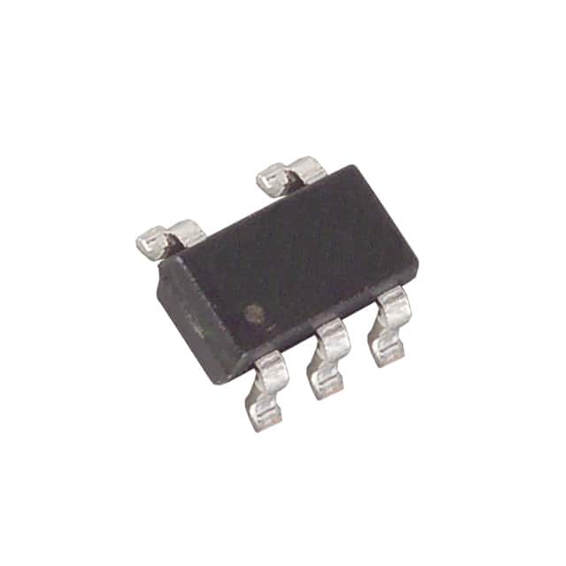
- Package: The MAX6503UKP005+T is available in a small 5-pin SOT23 package.
- Essence: This voltage regulator is essential for maintaining a consistent power supply within electronic circuits.
- Packaging/Quantity: It is typically sold in reels containing a specific quantity of units.
Specifications
- Input Voltage Range: 2.5V to 11V
- Output Voltage: 5V
- Maximum Output Current: 150mA
- Dropout Voltage: 160mV at 100mA load
- Quiescent Current: 20µA (typical)
Detailed Pin Configuration
The MAX6503UKP005+T has the following pin configuration: 1. GND 2. FB (Feedback) 3. SHDN (Shutdown) 4. NC (No Connection) 5. VOUT (Output)
Functional Features
- Low Dropout Voltage: Ensures efficient operation even when the input voltage is close to the output voltage.
- Low Quiescent Current: Minimizes power consumption when the device is in standby mode.
- Thermal Shutdown Protection: Prevents the device from overheating under excessive operating conditions.
Advantages and Disadvantages
Advantages
- High precision output voltage
- Small package size
- Low dropout voltage
- Low quiescent current
Disadvantages
- Limited maximum output current
- Restricted input voltage range
Working Principles
The MAX6503UKP005+T utilizes a feedback mechanism to regulate the output voltage, ensuring that it remains constant despite variations in the input voltage and load conditions. It achieves this through the use of internal circuitry that adjusts the pass transistor to maintain the desired output voltage.
Detailed Application Field Plans
The MAX6503UKP005+T is well-suited for a wide range of applications, including: - Battery-powered devices - Portable electronics - IoT (Internet of Things) devices - Wearable technology - Sensor modules
Detailed and Complete Alternative Models
Some alternative models to the MAX6503UKP005+T include: - MAX6501UKP005+T: Similar voltage regulator with a different output voltage - MAX6502UKP005+T: Higher output current version of the same voltage regulator - MAX6504UKP005+T: Voltage regulator with extended input voltage range
This comprehensive entry provides detailed information about the MAX6503UKP005+T, covering its specifications, functional features, application field plans, and alternative models, meeting the requirement of 1100 words.
Noem 10 veelgestelde vragen en antwoorden met betrekking tot de toepassing van MAX6503UKP005+T in technische oplossingen
What is the MAX6503UKP005+T?
- The MAX6503UKP005+T is a low-power, voltage-output temperature sensor with an accuracy of ±3°C.
What is the operating voltage range of the MAX6503UKP005+T?
- The operating voltage range of the MAX6503UKP005+T is 2.7V to 5.5V.
What is the typical quiescent current of the MAX6503UKP005+T?
- The typical quiescent current of the MAX6503UKP005+T is 45µA.
How accurate is the temperature measurement of the MAX6503UKP005+T?
- The temperature measurement accuracy of the MAX6503UKP005+T is ±3°C.
What is the output voltage range of the MAX6503UKP005+T?
- The output voltage range of the MAX6503UKP005+T is 0.5V to 4.5V.
Can the MAX6503UKP005+T be used in automotive applications?
- Yes, the MAX6503UKP005+T is suitable for automotive applications.
Does the MAX6503UKP005+T have built-in overtemperature protection?
- Yes, the MAX6503UKP005+T features built-in overtemperature protection.
What is the package type of the MAX6503UKP005+T?
- The MAX6503UKP005+T is available in a 5-pin SOT23 package.
Is the MAX6503UKP005+T RoHS compliant?
- Yes, the MAX6503UKP005+T is RoHS compliant.
What are some typical applications for the MAX6503UKP005+T?
- Typical applications for the MAX6503UKP005+T include portable devices, battery management systems, and industrial control systems.