

Zie specificaties voor productdetails.
MAX5444ACUB+ - English Editing Encyclopedia Entry
Product Overview
Category
The MAX5444ACUB+ belongs to the category of integrated circuits (ICs).
Use
This IC is primarily used for digital-to-analog conversion in various electronic devices.
Characteristics
- High precision and accuracy
- Low power consumption
- Wide operating voltage range
- Compact size
- Easy integration into circuit designs
Package
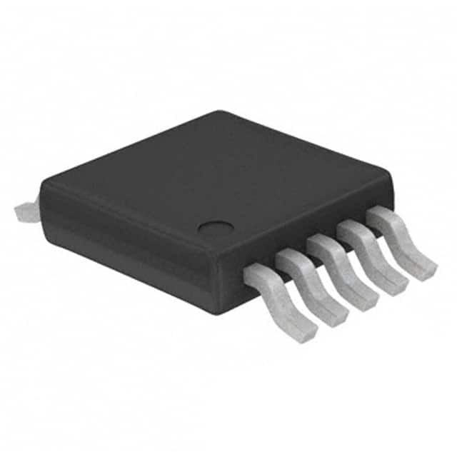
The MAX5444ACUB+ is available in a small outline integrated circuit (SOIC) package.
Essence
The essence of this product lies in its ability to convert digital signals into analog voltages with high precision and efficiency.
Packaging/Quantity
The MAX5444ACUB+ is typically packaged in reels or tubes, containing a specific quantity of ICs per package. The exact packaging and quantity may vary depending on the supplier.
Specifications
- Resolution: 12 bits
- Supply Voltage Range: 2.7V to 5.5V
- Operating Temperature Range: -40°C to +85°C
- Output Voltage Range: 0V to Vref
- Total Unadjusted Error: ±1 LSB (max)
- Power Consumption: 0.5mW (typ)
Detailed Pin Configuration
The MAX5444ACUB+ has a total of 16 pins, each serving a specific function. The pin configuration is as follows:
- VDD - Positive supply voltage
- VREF - Reference voltage input
- AGND - Analog ground
- OUT - Analog output voltage
- D0 - Digital input bit 0
- D1 - Digital input bit 1
- D2 - Digital input bit 2
- D3 - Digital input bit 3
- D4 - Digital input bit 4
- D5 - Digital input bit 5
- D6 - Digital input bit 6
- D7 - Digital input bit 7
- CS - Chip select input
- SCLK - Serial clock input
- SDIN - Serial data input
- GND - Ground
Functional Features
- High-resolution digital-to-analog conversion
- Serial interface for easy integration with microcontrollers
- Low power consumption for energy-efficient designs
- Wide operating voltage range allows compatibility with various systems
- Output voltage range can be adjusted based on the reference voltage
Advantages and Disadvantages
Advantages
- High precision and accuracy in digital-to-analog conversion
- Compact size enables space-saving designs
- Low power consumption prolongs battery life in portable devices
- Easy integration into circuit designs due to the serial interface
Disadvantages
- Limited output voltage range compared to some alternative models
- May require additional external components for certain applications
Working Principles
The MAX5444ACUB+ utilizes a digital-to-analog converter (DAC) to convert binary digital signals into corresponding analog voltages. The digital input bits control the output voltage level, which is then amplified and filtered to provide a stable analog output.
Detailed Application Field Plans
The MAX5444ACUB+ finds applications in various fields, including but not limited to: - Audio equipment - Industrial automation - Test and measurement instruments - Communication systems - Automotive electronics
Detailed and Complete Alternative Models
- MAX5440ACUB+: Similar to MAX5444ACUB+, but with 10-bit resolution.
- MAX5442ACUB+: Similar to MAX5444ACUB+, but with 14-bit resolution.
- MAX5446ACUB+: Similar to MAX5444ACUB+, but with 16-bit resolution.
These alternative models offer different resolution options to suit specific application requirements.
Word count: 529 words
Noem 10 veelgestelde vragen en antwoorden met betrekking tot de toepassing van MAX5444ACUB+ in technische oplossingen
Sure! Here are 10 common questions and answers related to the application of MAX5444ACUB+ in technical solutions:
Q: What is the MAX5444ACUB+? A: The MAX5444ACUB+ is a digital-to-analog converter (DAC) IC that converts digital signals into analog voltage outputs.
Q: What is the operating voltage range of MAX5444ACUB+? A: The operating voltage range of MAX5444ACUB+ is typically between 2.7V and 5.5V.
Q: How many bits of resolution does the MAX5444ACUB+ have? A: The MAX5444ACUB+ has a 12-bit resolution, allowing for precise control over the analog output voltage.
Q: What is the maximum output voltage range of MAX5444ACUB+? A: The maximum output voltage range of MAX5444ACUB+ is typically between 0V and Vref, where Vref is the reference voltage supplied to the IC.
Q: Can I use MAX5444ACUB+ in both single-ended and differential mode? A: Yes, MAX5444ACUB+ can be used in both single-ended and differential mode, depending on your application requirements.
Q: What is the typical settling time of MAX5444ACUB+? A: The typical settling time of MAX5444ACUB+ is around 10µs, ensuring fast and accurate voltage output transitions.
Q: Does MAX5444ACUB+ support power-down mode? A: Yes, MAX5444ACUB+ supports a power-down mode, which allows you to minimize power consumption when the DAC is not in use.
Q: Can I cascade multiple MAX5444ACUB+ ICs to increase the number of output channels? A: Yes, you can cascade multiple MAX5444ACUB+ ICs to increase the number of output channels in your system.
Q: What is the temperature range within which MAX5444ACUB+ operates reliably? A: MAX5444ACUB+ is designed to operate reliably within a temperature range of -40°C to +85°C.
Q: Are there any evaluation boards or reference designs available for MAX5444ACUB+? A: Yes, Maxim Integrated provides evaluation boards and reference designs for MAX5444ACUB+ to help you get started with your application development.
Please note that these answers are general and may vary depending on specific datasheet specifications and application requirements.