

Zie specificaties voor productdetails.
LFE2-35E-6F672I
Product Overview
Category
The LFE2-35E-6F672I belongs to the category of Field Programmable Gate Arrays (FPGAs).
Use
FPGAs are integrated circuits that can be programmed and reprogrammed to perform various digital functions. The LFE2-35E-6F672I is specifically designed for applications requiring high-performance and low-power consumption.
Characteristics
- High performance: The LFE2-35E-6F672I offers a combination of high-speed operation and efficient power utilization.
- Low power consumption: It is designed to minimize power usage, making it suitable for battery-powered devices.
- Programmability: The FPGA can be configured to implement custom logic functions, allowing for flexibility in design.
- Versatility: The LFE2-35E-6F672I supports a wide range of applications due to its programmable nature.
Package
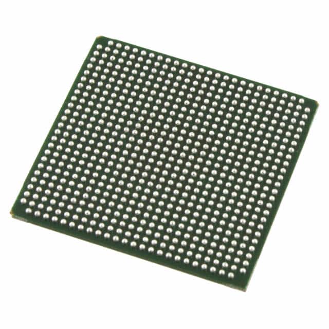
The LFE2-35E-6F672I comes in a compact package, ensuring easy integration into electronic systems. It is available in a surface-mount form factor.
Essence
The essence of the LFE2-35E-6F672I lies in its ability to provide high-performance digital functionality while consuming minimal power. Its programmability allows for customization, making it suitable for a variety of applications.
Packaging/Quantity
The LFE2-35E-6F672I is typically packaged in reels or trays, depending on the manufacturer's specifications. The quantity per package may vary, but it is commonly available in quantities of 100 or more.
Specifications
- FPGA Family: Lattice ECP2M
- Logic Elements: 35,000
- Speed Grade: -6
- Package Type: F672
- I/O Pins: 672
- Operating Voltage: 1.2V
- Operating Temperature Range: -40°C to +100°C
Detailed Pin Configuration
The LFE2-35E-6F672I has a total of 672 I/O pins, which are programmable and can be configured for various functions based on the application requirements. The pin configuration is detailed in the product datasheet provided by the manufacturer.
Functional Features
High-Speed Operation
The LFE2-35E-6F672I offers high-speed operation, allowing for efficient processing of digital signals. This makes it suitable for applications that require real-time data processing or high-speed communication.
Low-Power Consumption
With its low-power design, the LFE2-35E-6F672I minimizes energy consumption while maintaining optimal performance. This feature is particularly advantageous for battery-powered devices or applications where power efficiency is crucial.
Programmability
The FPGA's programmability enables users to implement custom logic functions tailored to their specific needs. This flexibility allows for rapid prototyping, design iterations, and easy adaptation to changing requirements.
Versatility
The LFE2-35E-6F672I supports a wide range of applications, including telecommunications, industrial automation, automotive electronics, and consumer electronics. Its versatility stems from its ability to be reprogrammed for different functionalities, making it adaptable to diverse use cases.
Advantages and Disadvantages
Advantages
- High-performance capabilities
- Low-power consumption
- Customizable logic functions
- Wide range of applications
Disadvantages
- Requires expertise in FPGA programming
- Higher cost compared to fixed-function integrated circuits
- Limited availability of alternative models with similar specifications
Working Principles
The LFE2-35E-6F672I operates based on the principles of field-programmable gate arrays. It consists of configurable logic blocks (CLBs), interconnect resources, and I/O blocks. The CLBs can be programmed to implement various logic functions, while the interconnect resources facilitate communication between different components within the FPGA. The I/O blocks provide interfaces for external connections.
Detailed Application Field Plans
The LFE2-35E-6F672I finds applications in various fields, including:
- Telecommunications: Used in network equipment, base stations, and communication protocols.
- Industrial Automation: Employed in control systems, robotics, and process automation.
- Automotive Electronics: Integrated into vehicle control units, infotainment systems, and driver assistance systems.
- Consumer Electronics: Utilized in high-definition displays, audio/video processing, and gaming consoles.
Detailed and Complete Alternative Models
While the LFE2-35E-6F672I offers unique features, there are alternative models available from other manufacturers that provide similar functionality. Some notable alternatives include:
- Xilinx Spartan-6 FPGA
- Intel (Altera) Cyclone IV FPGA
- Microsemi (Microchip) SmartFusion2 FPGA
These alternative models offer comparable performance, power efficiency, and programm
Noem 10 veelgestelde vragen en antwoorden met betrekking tot de toepassing van LFE2-35E-6F672I in technische oplossingen
Sure! Here are 10 common questions and answers related to the application of LFE2-35E-6F672I in technical solutions:
Q: What is the LFE2-35E-6F672I? A: The LFE2-35E-6F672I is a specific model of Field-Programmable Gate Array (FPGA) manufactured by Lattice Semiconductor.
Q: What are the key features of the LFE2-35E-6F672I? A: The key features of this FPGA include 35,000 Look-Up Tables (LUTs), 672 I/O pins, low power consumption, and high-speed performance.
Q: In what applications can the LFE2-35E-6F672I be used? A: This FPGA can be used in various applications such as industrial automation, telecommunications, automotive electronics, medical devices, and consumer electronics.
Q: How can the LFE2-35E-6F672I be programmed? A: The LFE2-35E-6F672I can be programmed using Hardware Description Languages (HDLs) like VHDL or Verilog, or through graphical programming tools provided by Lattice Semiconductor.
Q: What are the advantages of using the LFE2-35E-6F672I in technical solutions? A: Some advantages include its flexibility, reprogrammability, ability to handle complex logic functions, and faster time-to-market compared to custom ASIC designs.
Q: Can the LFE2-35E-6F672I interface with other components or devices? A: Yes, the FPGA can interface with various components and devices through its numerous I/O pins, allowing for seamless integration into larger systems.
Q: What is the power consumption of the LFE2-35E-6F672I? A: The power consumption of this FPGA depends on the specific design and usage, but it generally operates at low power levels to optimize energy efficiency.
Q: Can the LFE2-35E-6F672I handle high-speed data processing? A: Yes, this FPGA is designed to handle high-speed data processing with its advanced architecture and optimized routing capabilities.
Q: Are there any development tools or resources available for working with the LFE2-35E-6F672I? A: Yes, Lattice Semiconductor provides a range of development tools, software, and documentation to support designers working with their FPGAs, including design software and reference designs.
Q: Where can I find more information about the LFE2-35E-6F672I? A: You can find more detailed information about the LFE2-35E-6F672I on the official website of Lattice Semiconductor or by referring to the datasheet and technical documentation provided by the manufacturer.