

Zie specificaties voor productdetails.
EP3C10M164C7N
Product Overview
Category: Programmable Logic Device (PLD)
Use: The EP3C10M164C7N is a PLD that offers high-performance and low-power consumption for various digital logic applications. It provides designers with the flexibility to implement complex logic functions in a single device.
Characteristics: - High-performance: The EP3C10M164C7N operates at high clock frequencies, allowing for fast execution of logic functions. - Low-power consumption: This PLD is designed to minimize power consumption, making it suitable for battery-powered devices or energy-efficient applications. - Versatility: It supports a wide range of digital logic functions, including combinatorial and sequential circuits. - Scalability: The EP3C10M164C7N can be easily integrated into larger systems, thanks to its compatibility with other PLDs and microcontrollers. - Robustness: It offers reliable operation even in harsh environments, with built-in features for error detection and correction.
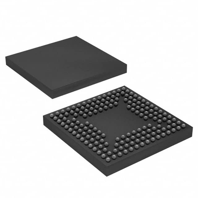
Package: The EP3C10M164C7N comes in a compact and durable package, ensuring easy handling and protection against external factors such as moisture and dust.
Essence: The essence of the EP3C10M164C7N lies in its ability to provide a flexible and efficient solution for implementing complex digital logic functions.
Packaging/Quantity: Each EP3C10M164C7N unit is packaged individually and is available in various quantities depending on the manufacturer's specifications.
Specifications
- Logic Elements: 10,080
- Memory Bits: 164,000
- Maximum User I/O Pins: 179
- Operating Voltage: 1.2V
- Operating Temperature Range: -40°C to 100°C
- Package Type: FBGA (Fine-pitch Ball Grid Array)
- Package Dimensions: 10mm x 10mm
Detailed Pin Configuration
The EP3C10M164C7N has a well-defined pin configuration that allows for easy integration into various circuit designs. The following table provides a detailed overview of the pin functions:
| Pin Number | Pin Name | Function | |------------|----------|----------| | 1 | VCCIO | I/O Power Supply Voltage | | 2 | GND | Ground | | 3 | IO0A | User I/O Pin | | 4 | IO0B | User I/O Pin | | ... | ... | ... | | 179 | IO178A | User I/O Pin | | 180 | IO178B | User I/O Pin | | ... | ... | ... |
Note: This is a simplified representation of the pin configuration. Please refer to the datasheet for the complete pinout details.
Functional Features
The EP3C10M164C7N offers several functional features that enhance its usability and performance:
- Programmability: It can be programmed using industry-standard hardware description languages (HDLs) such as VHDL or Verilog, allowing designers to implement custom logic functions.
- Embedded Memory: The PLD includes embedded memory blocks that can be used for storing data or implementing lookup tables.
- Clock Management: It supports advanced clock management techniques, including phase-locked loops (PLLs) for precise timing control.
- I/O Flexibility: The EP3C10M164C7N provides a wide range of I/O options, including differential signaling and support for various voltage levels.
- Security Features: It incorporates security features such as bitstream encryption and authentication to protect intellectual property and prevent unauthorized access.
Advantages and Disadvantages
Advantages: - High-performance and low-power consumption - Versatile and scalable design - Robust operation in harsh environments - Easy integration into larger systems - Secure programming and data protection
Disadvantages: - Limited logic elements compared to higher-end PLDs - Higher cost compared to simpler logic devices
Working Principles
The EP3C10M164C7N operates based on the principles of programmable logic. It consists of an array of configurable logic blocks (CLBs) interconnected through a programmable routing matrix. The CLBs can be configured to implement various logic functions, including combinatorial and sequential circuits.
During programming, the desired logic functions are defined using a hardware description language and synthesized into a configuration bitstream. This bitstream is then loaded into the EP3C10M164C7N, configuring the internal connections and functionality of the device.
Once programmed, the PLD executes the defined logic functions by routing signals through the interconnect matrix and performing the required operations within the CLBs. The output signals are then made available through the user I/O
Noem 10 veelgestelde vragen en antwoorden met betrekking tot de toepassing van EP3C10M164C7N in technische oplossingen
Sure! Here are 10 common questions and answers related to the application of EP3C10M164C7N in technical solutions:
Q: What is EP3C10M164C7N? A: EP3C10M164C7N is a field-programmable gate array (FPGA) manufactured by Intel. It offers 10,000 logic elements and is commonly used in various technical solutions.
Q: What are the key features of EP3C10M164C7N? A: Some key features of EP3C10M164C7N include 164 user I/O pins, embedded memory blocks, PLLs for clock management, and support for various communication protocols.
Q: In what applications can EP3C10M164C7N be used? A: EP3C10M164C7N can be used in a wide range of applications such as industrial automation, robotics, medical devices, automotive systems, and telecommunications.
Q: How can EP3C10M164C7N be programmed? A: EP3C10M164C7N can be programmed using hardware description languages (HDLs) like VHDL or Verilog, which are then synthesized into a bitstream file that can be loaded onto the FPGA.
Q: Can EP3C10M164C7N interface with other components or devices? A: Yes, EP3C10M164C7N supports various communication protocols like SPI, I2C, UART, and Ethernet, allowing it to interface with other components or devices in a system.
Q: What tools are available for designing with EP3C10M164C7N? A: Intel provides Quartus Prime software, which includes design entry, synthesis, simulation, and programming tools specifically tailored for designing with their FPGAs.
Q: Can EP3C10M164C7N be reprogrammed after deployment? A: Yes, EP3C10M164C7N is a reprogrammable FPGA, meaning its configuration can be changed even after it has been deployed in a system.
Q: What are the power requirements for EP3C10M164C7N? A: EP3C10M164C7N typically operates at a voltage range of 1.15V to 1.25V, and its power consumption depends on the design and utilization of the FPGA.
Q: Are there any limitations or considerations when using EP3C10M164C7N? A: Some considerations include the limited number of logic elements (10,000) and I/O pins (164), as well as the need for proper thermal management due to power dissipation.
Q: Where can I find more information about EP3C10M164C7N? A: You can find more detailed information, datasheets, reference designs, and application notes on Intel's website or by referring to the official documentation provided by Intel for EP3C10M164C7N.
Please note that the answers provided here are general and may vary depending on specific use cases and requirements.