

Zie specificaties voor productdetails.
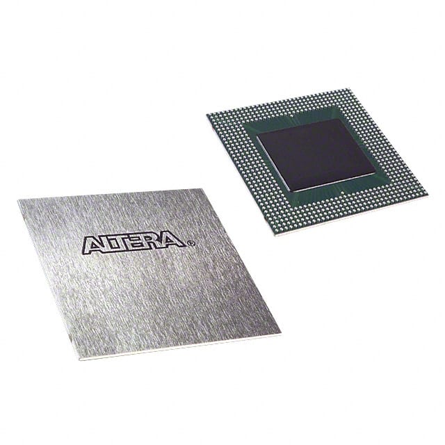
EP20K400CB652I8ES
Product Overview
- Category: Programmable Logic Device (PLD)
- Use: EP20K400CB652I8ES is a high-performance PLD designed for complex digital circuit designs.
- Characteristics:
- High logic capacity
- Fast performance
- Flexible and reprogrammable
- Package: The EP20K400CB652I8ES comes in a ceramic package.
- Essence: EP20K400CB652I8ES is an essential component for designing and implementing advanced digital circuits.
- Packaging/Quantity: The EP20K400CB652I8ES is typically sold individually.
Specifications
- Logic Capacity: 400,000 gates
- Speed Grade: 652 MHz
- I/O Pins: 652
- Operating Voltage: 3.3V
- Package Type: Ceramic BGA
- Temperature Range: -40°C to +85°C
Detailed Pin Configuration
The EP20K400CB652I8ES has a total of 652 pins, which are organized into various functional groups. The pin configuration includes:
- Power supply pins
- Ground pins
- Input/output pins
- Clock pins
- Configuration pins
- Special function pins
For a detailed pin configuration diagram, please refer to the product datasheet.
Functional Features
- High-density programmable logic device
- Advanced architecture for complex digital circuit designs
- Support for various I/O standards
- Built-in memory blocks for efficient implementation of complex algorithms
- On-chip clock management resources for precise timing control
- JTAG interface for easy programming and debugging
Advantages and Disadvantages
Advantages: - High logic capacity allows for complex circuit designs - Fast performance enables real-time processing - Reprogrammable nature provides flexibility for design changes - Wide temperature range for versatile applications - JTAG interface simplifies programming and debugging
Disadvantages: - Relatively high power consumption compared to other PLDs - Limited availability of alternative models with similar specifications
Working Principles
The EP20K400CB652I8ES is based on a complex programmable logic device architecture. It consists of an array of configurable logic blocks (CLBs), interconnect resources, I/O elements, and memory blocks. The CLBs can be programmed to implement various digital functions, while the interconnect resources allow for flexible routing of signals between different blocks. The I/O elements provide connectivity to external devices, and the memory blocks enable efficient implementation of complex algorithms.
The device is programmed using a hardware description language (HDL) such as VHDL or Verilog. The programming file is then loaded into the device using a programming tool, which configures the internal resources according to the desired circuit design. Once programmed, the EP20K400CB652I8ES operates as a dedicated digital circuit, executing the specified functions.
Detailed Application Field Plans
The EP20K400CB652I8ES finds applications in various fields, including:
- Telecommunications: Used in network routers, switches, and communication equipment for high-speed data processing.
- Industrial Automation: Employed in control systems, PLCs, and robotics for real-time control and monitoring.
- Automotive Electronics: Integrated into automotive control units, infotainment systems, and driver assistance systems.
- Aerospace and Defense: Utilized in avionics, radar systems, and military-grade electronics for reliable performance in harsh environments.
- Medical Devices: Incorporated into medical imaging systems, patient monitoring devices, and laboratory equipment.
Alternative Models
While the EP20K400CB652I8ES is a highly capable PLD, there are alternative models available with similar specifications. Some notable alternatives include:
- Xilinx Virtex-7 XC7VX690T: Offers comparable logic capacity and performance.
- Altera Stratix V 5SGXEA7N2F45C2: Provides similar features and capabilities.
- LatticeECP5 LFE5UM-85F-8BG381C: A lower-cost option with a slightly reduced logic capacity.
These alternative models can be considered based on specific project requirements and availability in the market.
Word count: 512 words
Noem 10 veelgestelde vragen en antwoorden met betrekking tot de toepassing van EP20K400CB652I8ES in technische oplossingen
Sure! Here are 10 common questions and answers related to the application of EP20K400CB652I8ES in technical solutions:
Q: What is EP20K400CB652I8ES? A: EP20K400CB652I8ES is a specific model of Field-Programmable Gate Array (FPGA) manufactured by Intel.
Q: What are the key features of EP20K400CB652I8ES? A: EP20K400CB652I8ES offers high-density programmable logic, embedded memory blocks, and various I/O options for flexible integration into technical solutions.
Q: In what technical applications can EP20K400CB652I8ES be used? A: EP20K400CB652I8ES can be used in a wide range of applications, including telecommunications, industrial automation, aerospace, and defense.
Q: How does EP20K400CB652I8ES enhance technical solutions? A: EP20K400CB652I8ES enhances technical solutions by providing customizable hardware acceleration, real-time processing capabilities, and improved system performance.
Q: Can EP20K400CB652I8ES be reprogrammed after deployment? A: Yes, EP20K400CB652I8ES is a field-programmable device, meaning it can be reprogrammed even after it has been deployed in a technical solution.
Q: What programming languages are supported for EP20K400CB652I8ES? A: EP20K400CB652I8ES supports popular hardware description languages (HDLs) such as VHDL and Verilog for programming and configuring its functionality.
Q: Are there any development tools available for EP20K400CB652I8ES? A: Yes, Intel provides development tools like Quartus Prime software suite that enables designers to program, simulate, and debug EP20K400CB652I8ES.
Q: What are the power requirements for EP20K400CB652I8ES? A: EP20K400CB652I8ES typically operates on a supply voltage of 3.3V or 2.5V, depending on the specific implementation.
Q: Can EP20K400CB652I8ES interface with other components in a technical solution? A: Yes, EP20K400CB652I8ES supports various communication protocols such as SPI, I2C, UART, and Ethernet, allowing it to interface with other components.
Q: Where can I find more information about EP20K400CB652I8ES? A: You can find detailed documentation, datasheets, and application notes on Intel's official website or by referring to the product manual provided with the FPGA.