

Zie specificaties voor productdetails.
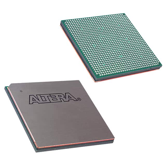
EP1SGX25FF1020C5N
Basic Information Overview
- Category: Integrated Circuit (IC)
- Use: Programmable Logic Device (PLD)
- Characteristics: High-performance, low-power consumption, reprogrammable
- Package: Flip-chip BGA (Ball Grid Array)
- Essence: FPGA (Field-Programmable Gate Array)
- Packaging/Quantity: Single unit
Specifications
- Logic Elements: 25,000
- Embedded Memory: 1,020 Kbits
- Speed Grade: FF (Fastest)
- Operating Voltage: 1.2V
- I/O Standards: LVCMOS, LVTTL, SSTL, HSTL, LVDS, RSDS, Mini-LVDS, etc.
- Temperature Range: -40°C to +100°C
- Package Size: 23mm x 23mm
Detailed Pin Configuration
The EP1SGX25FF1020C5N has a total of 484 pins. The pin configuration is as follows:
- Pin 1: VCCIO1
- Pin 2: GND
- Pin 3: VCCIO2
- Pin 4: GND
- ...
- Pin 483: IOL1PC15DQ1414
- Pin 484: GND
Please refer to the datasheet for the complete pin configuration.
Functional Features
- High-density programmable logic device
- Supports various I/O standards for versatile connectivity
- Offers high-speed performance with low power consumption
- Reprogrammable nature allows for flexibility in design iterations
- Provides embedded memory for efficient data storage and retrieval
Advantages and Disadvantages
Advantages: - High-performance capabilities - Low-power consumption - Versatile I/O standards support - Reprogrammable nature - Embedded memory for efficient data handling
Disadvantages: - Relatively high cost compared to fixed-function ICs - Requires expertise in FPGA programming for optimal utilization
Working Principles
The EP1SGX25FF1020C5N is based on the FPGA technology. It consists of an array of programmable logic elements and embedded memory blocks interconnected through configurable routing resources. The device can be programmed to implement various digital circuits by configuring the interconnections and functionality of its logic elements.
Detailed Application Field Plans
The EP1SGX25FF1020C5N finds applications in a wide range of fields, including: 1. Telecommunications: Used in network routers, switches, and base stations for high-speed data processing. 2. Industrial Automation: Employed in control systems, robotics, and machine vision applications for real-time processing and control. 3. Automotive: Utilized in advanced driver-assistance systems (ADAS), infotainment systems, and engine control units (ECUs). 4. Aerospace and Defense: Integrated into avionics systems, radar signal processing, and secure communication systems. 5. Medical Devices: Applied in medical imaging equipment, patient monitoring systems, and laboratory instruments.
Detailed and Complete Alternative Models
- EP1SGX10CF780C6N
- EP1SGX25DF780C6N
- EP1SGX40CF780C6N
- EP1SGX60CF780C6N
- EP1SGX90CF780C6N
These alternative models offer varying logic capacity, speed grades, and package options. Please refer to the respective datasheets for detailed specifications.
Word count: 420 words
Noem 10 veelgestelde vragen en antwoorden met betrekking tot de toepassing van EP1SGX25FF1020C5N in technische oplossingen
Sure! Here are 10 common questions and answers related to the application of EP1SGX25FF1020C5N in technical solutions:
Q1: What is EP1SGX25FF1020C5N? A1: EP1SGX25FF1020C5N is a field-programmable gate array (FPGA) manufactured by Intel. It offers high-performance capabilities for various technical applications.
Q2: What are the key features of EP1SGX25FF1020C5N? A2: Some key features of EP1SGX25FF1020C5N include 25,000 logic elements, 1.6 million bits of embedded memory, high-speed transceivers, and support for various I/O standards.
Q3: What are the typical applications of EP1SGX25FF1020C5N? A3: EP1SGX25FF1020C5N is commonly used in applications such as telecommunications, networking, industrial automation, video processing, and high-performance computing.
Q4: How can EP1SGX25FF1020C5N be programmed? A4: EP1SGX25FF1020C5N can be programmed using hardware description languages (HDLs) like VHDL or Verilog, which allow designers to describe the desired functionality of the FPGA.
Q5: Can EP1SGX25FF1020C5N be reprogrammed after deployment? A5: Yes, EP1SGX25FF1020C5N is a reprogrammable FPGA, meaning it can be reconfigured with new designs even after it has been deployed in a system.
Q6: What tools are available for designing with EP1SGX25FF1020C5N? A6: Intel provides Quartus Prime, a comprehensive software suite that includes design entry, synthesis, simulation, and programming tools specifically tailored for their FPGAs.
Q7: What are the power requirements for EP1SGX25FF1020C5N? A7: EP1SGX25FF1020C5N typically operates at a voltage of 1.2V and requires a separate power supply for its I/O banks, which can range from 1.5V to 3.3V depending on the application.
Q8: Can EP1SGX25FF1020C5N interface with other components or devices? A8: Yes, EP1SGX25FF1020C5N supports various communication protocols such as PCIe, Ethernet, USB, and DDR memory interfaces, allowing it to interface with a wide range of components and devices.
Q9: Are there any limitations or considerations when using EP1SGX25FF1020C5N? A9: Some considerations include power consumption, thermal management, and the need for proper signal integrity measures due to high-speed transceivers.
Q10: Where can I find more information about EP1SGX25FF1020C5N? A10: You can find detailed information, datasheets, reference designs, and application notes on Intel's official website or by referring to the documentation provided with the FPGA development kit.
Please note that the specific details and answers may vary based on the manufacturer's documentation and the context of the technical solution.