

Zie specificaties voor productdetails.
5SGXEB5R3F43I3L
Product Overview
- Category: Field Programmable Gate Array (FPGA)
- Use: Digital logic implementation, prototyping, and system integration
- Characteristics: High-performance, reconfigurable, programmable, and flexible
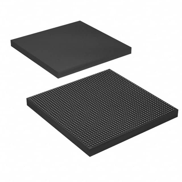
- Package: BGA (Ball Grid Array)
- Essence: Integrated circuit for customizable digital logic functions
- Packaging/Quantity: Single unit per package
Specifications
- Manufacturer: Intel Corporation
- Series: Stratix V
- Model: 5SGXEB5R3F43I3L
- Logic Elements: 462,000
- Embedded Memory: 34,816 Kbits
- DSP Blocks: 1,288
- Transceivers: 48
- I/O Pins: 1,040
- Operating Voltage: 0.87V - 0.93V
- Operating Temperature: -40°C to 100°C
- Package Type: F43 (1,151-pin BGA)
Detailed Pin Configuration
The 5SGXEB5R3F43I3L FPGA has a total of 1,040 I/O pins distributed across its package. The pin configuration includes various types of pins such as input, output, bidirectional, clock, and power pins. Each pin serves a specific purpose in the overall functionality of the FPGA.
For a detailed pin configuration diagram and description, please refer to the manufacturer's datasheet or documentation.
Functional Features
- High Performance: The 5SGXEB5R3F43I3L FPGA offers high-speed processing capabilities, making it suitable for demanding applications.
- Reconfigurability: The FPGA can be programmed and reprogrammed to implement different digital logic functions, allowing flexibility in system design.
- Integration: It enables the integration of multiple complex digital functions into a single chip, reducing the need for additional components.
- Customizability: The FPGA allows users to create custom logic circuits tailored to their specific requirements, providing design flexibility.
Advantages and Disadvantages
Advantages
- Flexibility: The reprogrammable nature of FPGAs allows for quick design iterations and modifications.
- High Performance: FPGAs can achieve high-speed processing due to their parallel architecture.
- Integration: Multiple functions can be combined into a single FPGA, reducing system complexity and cost.
- Prototyping: FPGAs are commonly used for rapid prototyping and proof-of-concept development.
Disadvantages
- Complexity: Designing for FPGAs requires specialized knowledge and expertise.
- Power Consumption: FPGAs can consume more power compared to fixed-function integrated circuits.
- Cost: FPGAs tend to be more expensive than off-the-shelf integrated circuits for large-scale production.
Working Principles
The 5SGXEB5R3F43I3L FPGA operates based on the principles of configurable logic blocks (CLBs) and interconnect resources. CLBs consist of look-up tables (LUTs), flip-flops, and multiplexers, which can be configured to implement various logic functions. Interconnect resources provide routing paths between different CLBs, allowing signals to flow through the FPGA.
During operation, the FPGA is programmed using a hardware description language (HDL) or a graphical user interface (GUI). The programming defines the desired logic functions and interconnections within the FPGA. Once programmed, the FPGA executes the specified logic operations, enabling the desired functionality.
Detailed Application Field Plans
The 5SGXEB5R3F43I3L FPGA finds applications in various fields, including:
- Telecommunications: Used for signal processing, protocol implementation, and network infrastructure.
- Aerospace and Defense: Employed in radar systems, avionics, and secure communication systems.
- High-Performance Computing: Utilized for data acceleration, parallel processing, and algorithm acceleration.
- Industrial Automation: Applied in control systems, robotics, and machine vision applications.
- Medical Devices: Used for image processing, diagnostics, and real-time monitoring.
Detailed and Complete Alternative Models
- 5SGXEB5R2F43I3L: Similar to 5SGXEB5R3F43I3L but with a lower number of logic elements.
- 5SGXEB5R4F43I3L: Similar to 5SGXEB5R3F43I3L but with a higher number of logic elements.
- 5SGXEB5R3F40I3L: Similar to 5SGXEB5R3F43I3L but with a different package type.
These alternative models offer varying specifications and may be suitable for different application requirements.
*Note: The content provided above is a general overview and may not cover all aspects of the product. For
Noem 10 veelgestelde vragen en antwoorden met betrekking tot de toepassing van 5SGXEB5R3F43I3L in technische oplossingen
Sure! Here are 10 common questions and answers related to the application of 5SGXEB5R3F43I3L in technical solutions:
Q: What is the 5SGXEB5R3F43I3L FPGA used for? A: The 5SGXEB5R3F43I3L is a Field-Programmable Gate Array (FPGA) that can be used for various applications such as high-performance computing, networking, and signal processing.
Q: What are the key features of the 5SGXEB5R3F43I3L FPGA? A: Some key features of this FPGA include a large number of logic elements, high-speed transceivers, embedded memory blocks, and support for various communication protocols.
Q: Can the 5SGXEB5R3F43I3L FPGA be used for real-time video processing? A: Yes, the high-performance capabilities of this FPGA make it suitable for real-time video processing applications like video encoding, decoding, and image recognition.
Q: Is the 5SGXEB5R3F43I3L FPGA suitable for high-bandwidth networking applications? A: Absolutely, this FPGA offers high-speed transceivers that enable it to handle high-bandwidth networking tasks such as data packet routing and switching.
Q: Can the 5SGXEB5R3F43I3L FPGA be used for implementing cryptographic algorithms? A: Yes, this FPGA supports hardware acceleration for cryptographic algorithms, making it suitable for applications requiring secure data encryption and decryption.
Q: Does the 5SGXEB5R3F43I3L FPGA support PCIe connectivity? A: Yes, this FPGA has built-in support for PCIe (Peripheral Component Interconnect Express) connectivity, allowing it to interface with other devices using this standard.
Q: What development tools are available for programming the 5SGXEB5R3F43I3L FPGA? A: The 5SGXEB5R3F43I3L can be programmed using Intel Quartus Prime software, which provides a comprehensive suite of design and verification tools.
Q: Can the 5SGXEB5R3F43I3L FPGA be used in safety-critical applications? A: Yes, this FPGA offers features like error correction codes (ECC) and redundancy mechanisms that make it suitable for safety-critical applications such as aerospace or automotive systems.
Q: Is the 5SGXEB5R3F43I3L FPGA compatible with other FPGA families from Intel? A: Yes, this FPGA is part of the Intel Stratix 5 family, and it is compatible with other members of the same family, allowing for easy migration between different FPGA models.
Q: Are there any reference designs or application notes available for the 5SGXEB5R3F43I3L FPGA? A: Yes, Intel provides a wide range of reference designs and application notes that can help developers get started with implementing solutions using the 5SGXEB5R3F43I3L FPGA.
Please note that the specific details and answers may vary depending on the context and requirements of the technical solution being developed.