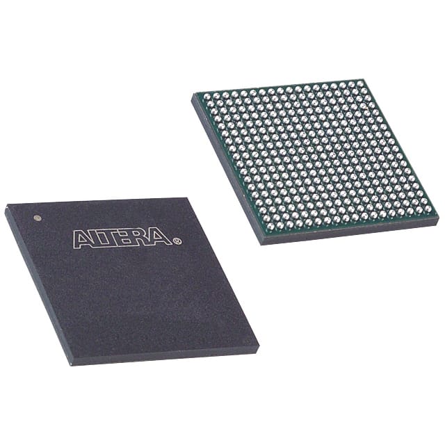
Zie specificaties voor productdetails.

5CGXBC3B6U15C7N
Product Overview
Category
The 5CGXBC3B6U15C7N belongs to the category of Field Programmable Gate Arrays (FPGAs).
Use
FPGAs are integrated circuits that can be programmed and reprogrammed to perform various digital functions. The 5CGXBC3B6U15C7N is specifically designed for high-performance applications.
Characteristics
- High-performance FPGA with advanced features
- Flexible and reprogrammable design
- Supports complex digital logic functions
- Offers high-speed data processing capabilities
- Suitable for demanding applications requiring real-time processing
Package
The 5CGXBC3B6U15C7N comes in a compact package, ensuring easy integration into electronic systems.
Essence
The essence of the 5CGXBC3B6U15C7N lies in its ability to provide customizable digital logic functionality, enabling designers to implement complex algorithms and processing tasks efficiently.
Packaging/Quantity
The 5CGXBC3B6U15C7N is typically packaged individually and is available in various quantities depending on the manufacturer's specifications.
Specifications
- FPGA Family: Cyclone V GX
- Logic Elements: 5,200
- Embedded Memory: 414 Kbits
- DSP Blocks: 96
- Maximum User I/Os: 266
- Operating Voltage: 1.2V
- Speed Grade: 6
- Package Type: FBGA
- Package Pins: 484
Detailed Pin Configuration
The detailed pin configuration of the 5CGXBC3B6U15C7N can be found in the manufacturer's datasheet or technical documentation.
Functional Features
- High-speed data processing capabilities
- Configurable logic elements for custom functionality
- Embedded memory for data storage
- Digital Signal Processing (DSP) blocks for efficient signal processing
- Support for various communication protocols and interfaces
- On-chip peripherals for system integration
Advantages and Disadvantages
Advantages
- Flexibility: The FPGA can be reprogrammed to adapt to changing requirements.
- High Performance: The 5CGXBC3B6U15C7N offers high-speed data processing capabilities.
- Customizability: The FPGA allows designers to implement complex algorithms and functions.
- Integration: On-chip peripherals enable seamless integration into electronic systems.
Disadvantages
- Complexity: Designing with FPGAs requires specialized knowledge and expertise.
- Power Consumption: FPGAs can consume more power compared to dedicated ASICs.
- Cost: FPGAs can be more expensive than other integrated circuits for certain applications.
Working Principles
The 5CGXBC3B6U15C7N operates based on the principles of reconfigurable digital logic. It consists of configurable logic elements, embedded memory, and DSP blocks that can be programmed to perform specific tasks. The FPGA is configured using a Hardware Description Language (HDL), which defines the desired functionality. Upon configuration, the FPGA executes the programmed logic, enabling the desired digital processing.
Detailed Application Field Plans
The 5CGXBC3B6U15C7N finds applications in various fields, including:
- Telecommunications: Used in high-speed data transmission systems and network infrastructure equipment.
- Aerospace and Defense: Employed in radar systems, avionics, and military communication systems.
- Industrial Automation: Utilized in control systems, robotics, and machine vision applications.
- Medical Devices: Integrated into medical imaging systems, patient monitoring devices, and diagnostic equipment.
- Automotive: Applied in advanced driver-assistance systems (ADAS), infotainment systems, and engine control units.
Detailed and Complete Alternative Models
- 5CGXFC7D6F27C8N
- 5CGXFC9E7F31C8N
- 5CGXFC5C6F27C8N
- 5CGXFC7C6F27C8N
- 5CGXFC9C6F27C8N
These alternative models offer similar functionality and performance to the 5CGXBC3B6U15C7N and can be considered as alternatives based on specific project requirements.
Note: The above information is provided for reference purposes only. For accurate and up-to-date details, please refer to the manufacturer's documentation.
Noem 10 veelgestelde vragen en antwoorden met betrekking tot de toepassing van 5CGXBC3B6U15C7N in technische oplossingen
Sure! Here are 10 common questions and answers related to the application of 5CGXBC3B6U15C7N in technical solutions:
Q: What is the 5CGXBC3B6U15C7N FPGA used for? A: The 5CGXBC3B6U15C7N is a Field-Programmable Gate Array (FPGA) that can be used for various applications, including digital signal processing, high-speed communication, and embedded systems.
Q: What is the maximum number of logic elements in the 5CGXBC3B6U15C7N? A: The 5CGXBC3B6U15C7N has a maximum of 6,000 logic elements (LEs).
Q: Can the 5CGXBC3B6U15C7N support high-speed communication protocols? A: Yes, the 5CGXBC3B6U15C7N supports various high-speed communication protocols such as PCIe, Ethernet, and USB.
Q: What is the operating voltage range of the 5CGXBC3B6U15C7N? A: The 5CGXBC3B6U15C7N operates at a voltage range of 0.87V to 1.15V.
Q: Does the 5CGXBC3B6U15C7N have built-in memory? A: No, the 5CGXBC3B6U15C7N does not have built-in memory. However, it can interface with external memory devices.
Q: Can I reprogram the 5CGXBC3B6U15C7N after it has been configured? A: Yes, the 5CGXBC3B6U15C7N is a reprogrammable FPGA, allowing you to modify its configuration even after it has been programmed.
Q: What development tools are available for programming the 5CGXBC3B6U15C7N? A: The 5CGXBC3B6U15C7N can be programmed using Intel Quartus Prime software, which provides a comprehensive development environment.
Q: Can the 5CGXBC3B6U15C7N interface with other components or devices? A: Yes, the 5CGXBC3B6U15C7N supports various interfaces such as GPIO, I2C, SPI, and UART, allowing it to communicate with other components or devices.
Q: What is the maximum operating frequency of the 5CGXBC3B6U15C7N? A: The maximum operating frequency of the 5CGXBC3B6U15C7N depends on the specific design and implementation, but it can typically reach frequencies in the range of hundreds of megahertz (MHz) to gigahertz (GHz).
Q: Are there any reference designs or application notes available for the 5CGXBC3B6U15C7N? A: Yes, Intel provides reference designs and application notes that can help you get started with the 5CGXBC3B6U15C7N and understand its various applications and capabilities.
Please note that the answers provided here are general and may vary depending on the specific requirements and use cases. It's always recommended to refer to the official documentation and datasheets for accurate and up-to-date information.

