

Zie specificaties voor productdetails.
Encyclopedia Entry: 74SSTVF16859PAG8
Product Overview
Category
The 74SSTVF16859PAG8 belongs to the category of integrated circuits (ICs) and specifically falls under the family of voltage level translators.
Use
This product is primarily used for bidirectional voltage level translation between two different voltage domains. It enables seamless communication between devices operating at different voltage levels, ensuring compatibility and reliable data transfer.
Characteristics
- Bidirectional voltage level translation
- Supports multiple voltage domains
- High-speed operation
- Low power consumption
- Compact package size
- Robust design for reliable performance
Package and Quantity
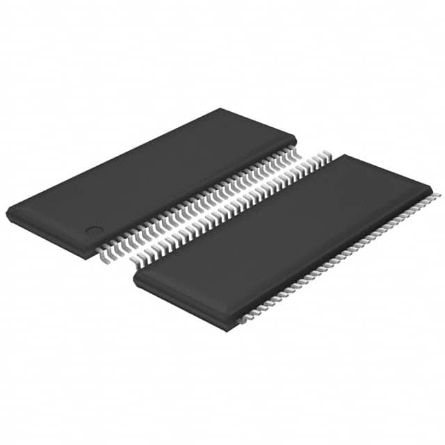
The 74SSTVF16859PAG8 is available in a small form factor package, such as a 56-pin TSSOP (Thin Shrink Small Outline Package). Each package contains one unit of the IC.
Specifications
- Supply Voltage Range: 1.2V to 3.6V
- Input Voltage Range (A Port): 0V to VCCA + 0.5V
- Input Voltage Range (B Port): 0V to VCCB + 0.5V
- Output Voltage Range (A Port): 0V to VCCA + 0.5V
- Output Voltage Range (B Port): 0V to VCCB + 0.5V
- Maximum Data Rate: 400 Mbps
- Operating Temperature Range: -40°C to +85°C
Pin Configuration
The 74SSTVF16859PAG8 has a total of 56 pins arranged in a specific configuration. The detailed pinout diagram can be found in the product datasheet.
Functional Features
- Bidirectional voltage level translation between two voltage domains
- Automatic direction sensing and control
- Support for high-speed data transmission
- Built-in ESD protection for enhanced reliability
- Low power consumption for energy-efficient operation
Advantages
- Enables seamless communication between devices operating at different voltage levels
- High-speed operation allows for efficient data transfer
- Compact package size saves board space
- Robust design ensures reliable performance even in challenging environments
- Automatic direction sensing simplifies system design
Disadvantages
- Limited to a specific number of voltage domains
- May require additional external components for certain applications
- Higher cost compared to simpler level shifting solutions
Working Principles
The 74SSTVF16859PAG8 utilizes a combination of level shifting techniques, such as voltage translation circuits and bidirectional buffers, to achieve bidirectional voltage level translation. It automatically senses the direction of data flow and adjusts the voltage levels accordingly, ensuring seamless communication between devices.
Application Field Plans
The 74SSTVF16859PAG8 finds extensive use in various application fields, including: 1. Communication systems 2. Data storage devices 3. Industrial automation 4. Automotive electronics 5. Consumer electronics
Alternative Models
For users seeking alternative options, the following models provide similar functionality: 1. 74LVC245: Low-voltage octal bus transceiver with direction control 2. SN74LV1T34: Single-bit dual-supply bus buffer gate 3. TXB0108: 8-bit bidirectional voltage-level translator
These alternative models offer comparable features and can be considered based on specific requirements.
In conclusion, the 74SSTVF16859PAG8 is a versatile integrated circuit that facilitates bidirectional voltage level translation between different voltage domains. Its high-speed operation, compact package size, and robust design make it suitable for a wide range of applications. However, users should consider alternative models depending on their specific needs.
Noem 10 veelgestelde vragen en antwoorden met betrekking tot de toepassing van 74SSTVF16859PAG8 in technische oplossingen
Sure! Here are 10 common questions and answers related to the application of 74SSTVF16859PAG8 in technical solutions:
Q: What is the 74SSTVF16859PAG8? A: The 74SSTVF16859PAG8 is a high-speed, low-voltage, 20-bit universal bus transceiver with 3-state outputs.
Q: What is the operating voltage range for the 74SSTVF16859PAG8? A: The operating voltage range for this device is typically between 1.2V and 3.6V.
Q: What is the maximum data rate supported by the 74SSTVF16859PAG8? A: The maximum data rate supported by this device is typically up to 400 Mbps.
Q: Can the 74SSTVF16859PAG8 be used in both input and output applications? A: Yes, this device can be used as both an input and output buffer in various applications.
Q: What is the purpose of the 3-state outputs in the 74SSTVF16859PAG8? A: The 3-state outputs allow multiple devices to share a common bus without interfering with each other.
Q: Does the 74SSTVF16859PAG8 support hot-swapping capability? A: No, this device does not support hot-swapping capability. It is recommended to power down the device before connecting or disconnecting it from the bus.
Q: Can the 74SSTVF16859PAG8 be used in high-speed communication systems? A: Yes, this device is designed for high-speed applications and can be used in various communication systems.
Q: What is the typical power consumption of the 74SSTVF16859PAG8? A: The typical power consumption of this device is low, making it suitable for power-sensitive applications.
Q: Does the 74SSTVF16859PAG8 have built-in ESD protection? A: Yes, this device typically includes built-in ESD protection to safeguard against electrostatic discharge.
Q: Are there any specific layout guidelines to consider when using the 74SSTVF16859PAG8? A: Yes, it is recommended to follow the layout guidelines provided in the datasheet to ensure optimal performance and minimize signal integrity issues.
Please note that the answers provided here are general and may vary depending on the specific application and requirements. It is always advisable to refer to the datasheet or consult with the manufacturer for detailed information.