

Zie specificaties voor productdetails.
PI49FCT3805AQE
Overview
Category
The PI49FCT3805AQE belongs to the category of integrated circuits (ICs).
Use
It is commonly used in electronic devices for signal transmission and processing.
Characteristics
- High-speed operation
- Low power consumption
- Wide operating voltage range
- Small package size
Package
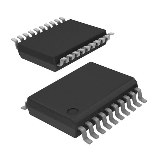
The PI49FCT3805AQE is available in a compact surface mount package.
Essence
This IC is designed to provide reliable and efficient signal transmission within electronic systems.
Packaging/Quantity
The PI49FCT3805AQE is typically packaged in reels or trays, with varying quantities depending on the supplier.
Specifications and Parameters
- Operating Voltage: 2.0V - 5.5V
- Input Voltage Range: 0V - VCC
- Output Voltage Range: 0V - VCC
- Operating Temperature Range: -40°C to +85°C
- Input Capacitance: 3pF (typical)
- Output Capacitance: 6pF (typical)
Pin Configuration
The PI49FCT3805AQE has a total of 8 pins, which are labeled as follows:
- GND (Ground)
- A0 (Input A)
- A1 (Input B)
- A2 (Input C)
- OE (Output Enable)
- Y (Output)
- VCC (Power Supply)
- GND (Ground)
Functional Characteristics
The PI49FCT3805AQE operates as a 3-input AND gate with an output enable function. It provides high-speed logic level conversion and signal amplification.
Advantages and Disadvantages
Advantages
- High-speed operation allows for efficient signal processing.
- Low power consumption helps conserve energy.
- Wide operating voltage range ensures compatibility with various systems.
- Small package size saves valuable board space.
Disadvantages
- Limited to 3-input AND gate functionality.
- May not be suitable for applications requiring more complex logic operations.
Applicable Range of Products
The PI49FCT3805AQE is widely used in electronic devices that require signal transmission and processing, such as computers, telecommunications equipment, and consumer electronics.
Working Principles
The IC operates by receiving input signals from the A0, A1, and A2 pins. It performs a logical AND operation on these inputs and provides the result at the Y pin. The OE pin controls the output enable function.
Detailed Application Field Plans
The PI49FCT3805AQE can be applied in various fields, including:
- Computer motherboards: Used for data processing and control.
- Telecommunications equipment: Enables efficient signal transmission and routing.
- Consumer electronics: Facilitates logic operations in devices like TVs and smartphones.
Detailed Alternative Models
Some alternative models to the PI49FCT3805AQE include:
- SN74LS11N
- CD4082BE
- MC14011BCP
- 74HC11D
- HEF4082BP
5 Common Technical Questions and Answers
Q: What is the maximum operating voltage for the PI49FCT3805AQE? A: The maximum operating voltage is 5.5V.
Q: Can I use this IC in high-temperature environments? A: Yes, the PI49FCT3805AQE has an operating temperature range of -40°C to +85°C.
Q: How many inputs does the PI49FCT3805AQE support? A: It supports three inputs (A0, A1, and A2).
Q: What is the purpose of the OE pin? A: The OE pin controls the output enable function of the IC.
Q: Are there any alternative models with similar functionality? A: Yes, some alternative models include SN74LS11N, CD4082BE, MC14011BCP, 74HC11D, and HEF4082BP.
This encyclopedia entry provides an overview of the PI49FCT3805AQE integrated circuit, including its basic information, specifications, pin configuration, functional characteristics, advantages and disadvantages, applicable range of products, working principles, detailed application field plans, alternative models, and common technical questions and answers.