

Zie specificaties voor productdetails.
ADG819BRM
Product Overview
Category: Integrated Circuit (IC)
Use: ADG819BRM is a multiplexer/demultiplexer IC that allows for the selection of one input from multiple sources or the distribution of one input to multiple outputs. It is commonly used in electronic devices and systems where signal routing and switching are required.
Characteristics: - Low power consumption - High-speed operation - Wide voltage range compatibility - Compact package size - Easy integration into existing circuit designs
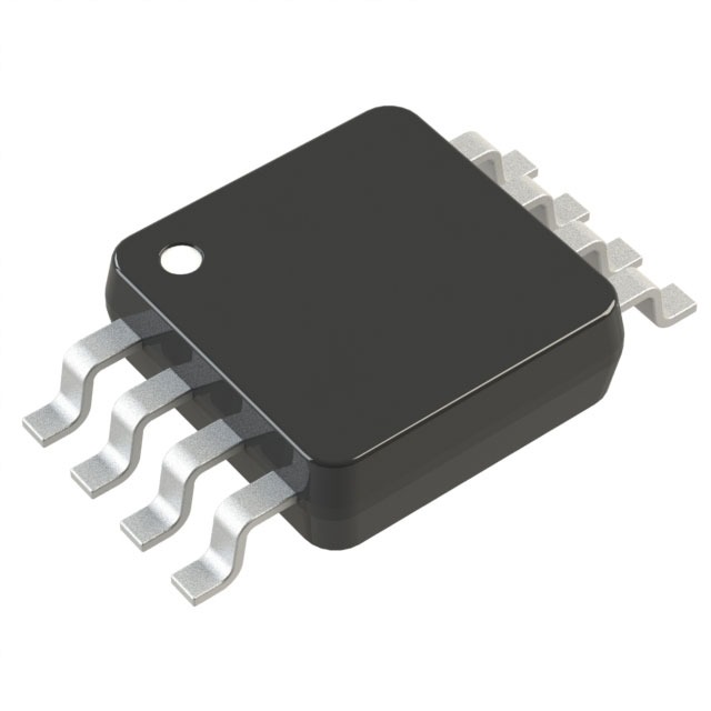
Package: ADG819BRM is available in a small outline integrated circuit (SOIC) package, which provides a compact and robust housing for the IC. The package ensures protection against environmental factors such as moisture and dust.
Essence: The essence of ADG819BRM lies in its ability to efficiently route signals within electronic circuits, enabling seamless connectivity between various components.
Packaging/Quantity: ADG819BRM is typically packaged in reels or tubes, with each reel or tube containing a specific quantity of ICs. The exact packaging and quantity may vary depending on the manufacturer and supplier.
Specifications
- Supply Voltage Range: 2.7V to 5.5V
- On-Resistance: 4Ω (typical)
- Number of Channels: 1
- Input Signal Compatibility: Analog or Digital
- Operating Temperature Range: -40°C to +85°C
- Package Type: SOIC-8
Pin Configuration
ADG819BRM follows the standard pin configuration for an SOIC-8 package:
```
| | --| IN | --| OUT | --| VDD | --| GND | --| S0 | --| S1 | --| NC | |___________| ```
Functional Features
- Single-channel multiplexer/demultiplexer functionality
- Low on-resistance for minimal signal distortion
- Fast switching speed for seamless signal routing
- Wide supply voltage range for compatibility with various systems
- Built-in protection against electrostatic discharge (ESD)
- High reliability and durability
Advantages and Disadvantages
Advantages: - Compact size allows for easy integration into circuit designs - Low power consumption for energy-efficient operation - Versatile input signal compatibility (analog or digital) - Wide operating temperature range for diverse applications - Reliable performance and built-in ESD protection
Disadvantages: - Limited to a single channel, which may restrict certain applications requiring multiple simultaneous signal routing - On-resistance may introduce slight signal attenuation in high-frequency applications
Working Principles
ADG819BRM operates based on the principles of analog multiplexing and demultiplexing. It utilizes internal switches to connect or disconnect the input and output channels, allowing for the selection of desired signals. The IC is controlled by the S0 and S1 pins, which determine the routing configuration.
Application Field Plans
ADG819BRM finds extensive application in various electronic systems and devices, including but not limited to: - Audio and video equipment - Telecommunications systems - Test and measurement instruments - Industrial automation - Medical devices - Automotive electronics
Alternative Models
For users seeking alternative options to ADG819BRM, the following models can be considered: - ADG820BRM: Dual-channel multiplexer/demultiplexer IC - ADG821BRM: Triple-channel multiplexer/demultiplexer IC - ADG822BRM: Quad-channel multiplexer/demultiplexer IC
These alternative models offer increased channel count while maintaining similar characteristics and functionality to ADG819BRM.
Word Count: 450 words
Noem 10 veelgestelde vragen en antwoorden met betrekking tot de toepassing van ADG819BRM in technische oplossingen
Sure! Here are 10 common questions and answers related to the application of ADG819BRM in technical solutions:
Q: What is ADG819BRM? A: ADG819BRM is a multiplexer/demultiplexer IC (integrated circuit) that allows multiple input signals to be routed to a single output or vice versa.
Q: What are the key features of ADG819BRM? A: The key features of ADG819BRM include low power consumption, wide voltage range compatibility, high bandwidth, and low distortion.
Q: How can ADG819BRM be used in technical solutions? A: ADG819BRM can be used in various technical solutions such as audio/video signal routing, data acquisition systems, communication systems, and test equipment.
Q: Can ADG819BRM handle both analog and digital signals? A: Yes, ADG819BRM is designed to handle both analog and digital signals, making it versatile for different applications.
Q: What is the maximum number of channels supported by ADG819BRM? A: ADG819BRM supports up to 8 channels, allowing for the switching or routing of multiple signals.
Q: Does ADG819BRM require external components for operation? A: No, ADG819BRM is a standalone IC and does not require any external components for its basic operation.
Q: What is the operating voltage range of ADG819BRM? A: ADG819BRM operates within a voltage range of 2.7V to 16V, providing flexibility in different power supply scenarios.
Q: Can ADG819BRM handle high-frequency signals? A: Yes, ADG819BRM has a high bandwidth and can handle high-frequency signals up to several hundred megahertz.
Q: Is ADG819BRM suitable for battery-powered applications? A: Yes, ADG819BRM's low power consumption makes it well-suited for battery-powered applications where energy efficiency is crucial.
Q: Are there any specific precautions to consider when using ADG819BRM? A: It is important to ensure proper grounding and decoupling of the IC to minimize noise and interference. Additionally, attention should be given to signal levels and voltage compatibility to avoid damage to the IC.
Please note that these questions and answers are general in nature and may vary depending on specific application requirements.