

Zie specificaties voor productdetails.
ADCMP670-1YUJZ-RL7
Product Overview
Category
The ADCMP670-1YUJZ-RL7 belongs to the category of analog-to-digital converters (ADCs).
Use
This product is primarily used for converting analog signals into digital format, enabling accurate and precise measurements in various applications.
Characteristics
- High resolution: The ADCMP670-1YUJZ-RL7 offers a high-resolution conversion, ensuring accurate representation of analog signals.
- Fast conversion speed: With its fast conversion rate, this ADC can handle real-time data acquisition requirements.
- Low power consumption: The device is designed to operate efficiently with low power consumption, making it suitable for battery-powered applications.
- Wide input voltage range: The ADCMP670-1YUJZ-RL7 can handle a wide range of input voltages, allowing flexibility in signal acquisition.
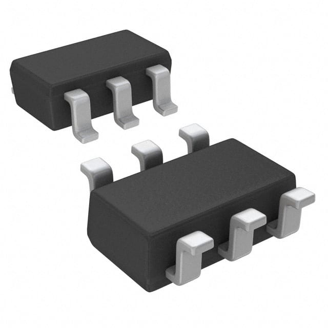
Package and Quantity
The ADCMP670-1YUJZ-RL7 is available in a compact surface-mount package. Each package contains one unit of the ADC.
Specifications
- Resolution: 12 bits
- Conversion Rate: 1 MSPS (Mega Samples Per Second)
- Input Voltage Range: ±5V
- Power Supply: 3.3V
- Operating Temperature Range: -40°C to +85°C
Pin Configuration
The ADCMP670-1YUJZ-RL7 has the following pin configuration:
| Pin Number | Pin Name | Description | |------------|----------|-------------| | 1 | VDD | Power supply voltage | | 2 | VREF | Reference voltage input | | 3 | VIN+ | Positive analog input | | 4 | VIN- | Negative analog input | | 5 | CLK | Clock input | | 6 | CS | Chip select input | | 7 | DOUT | Digital output | | 8 | GND | Ground |
Functional Features
- High accuracy: The ADCMP670-1YUJZ-RL7 provides accurate conversion results, ensuring reliable data acquisition.
- Low noise: The device is designed to minimize noise interference, resulting in clean and precise digital outputs.
- Flexible interface: It supports various communication interfaces, allowing easy integration into different systems.
- Built-in reference voltage: The ADC includes an internal reference voltage, eliminating the need for an external reference source.
Advantages
- High-resolution conversion enables precise measurements.
- Fast conversion rate allows real-time data acquisition.
- Low power consumption extends battery life in portable applications.
- Wide input voltage range accommodates diverse signal levels.
Disadvantages
- Limited resolution compared to higher-end ADCs.
- May require additional circuitry for specific applications with specialized requirements.
Working Principles
The ADCMP670-1YUJZ-RL7 utilizes a successive approximation register (SAR) architecture. It samples the analog input voltage, compares it to a reference voltage, and generates a digital representation of the input signal using a binary search algorithm.
Detailed Application Field Plans
The ADCMP670-1YUJZ-RL7 finds applications in various fields, including: 1. Industrial automation: Precise measurement of sensor signals in control systems. 2. Medical devices: Accurate data acquisition in patient monitoring equipment. 3. Test and measurement instruments: High-resolution signal analysis and data logging. 4. Communication systems: Analog-to-digital conversion for signal processing and modulation.
Alternative Models
For alternative options, consider the following ADCs: 1. ADCMP680-1YUJZ-RL7: A higher-resolution ADC with 16-bit conversion capability. 2. ADCMP690-1YUJZ-RL7: A lower-resolution ADC with 10-bit conversion capability. 3. ADCMP660-1YUJZ-RL7: A similar 12-bit ADC with a different pin configuration.
In conclusion, the ADCMP670-1YUJZ-RL7 is a high-resolution analog-to-digital converter that offers fast conversion speed, low power consumption, and wide input voltage range. Its accurate measurements and flexible interface make it suitable for various applications in industrial automation, medical devices, test and measurement instruments, and communication systems.
Noem 10 veelgestelde vragen en antwoorden met betrekking tot de toepassing van ADCMP670-1YUJZ-RL7 in technische oplossingen
Sure! Here are 10 common questions and answers related to the application of ADCMP670-1YUJZ-RL7 in technical solutions:
Q1: What is the ADCMP670-1YUJZ-RL7? A1: The ADCMP670-1YUJZ-RL7 is a high-speed comparator integrated circuit (IC) that can be used in various technical solutions.
Q2: What is the operating voltage range of ADCMP670-1YUJZ-RL7? A2: The ADCMP670-1YUJZ-RL7 operates within a voltage range of 2.7V to 5.5V.
Q3: What is the typical response time of ADCMP670-1YUJZ-RL7? A3: The typical response time of ADCMP670-1YUJZ-RL7 is around 4 ns.
Q4: Can ADCMP670-1YUJZ-RL7 be used in low-power applications? A4: Yes, ADCMP670-1YUJZ-RL7 has a low power consumption and can be used in low-power applications.
Q5: What is the input voltage range of ADCMP670-1YUJZ-RL7? A5: The input voltage range of ADCMP670-1YUJZ-RL7 is from -0.3V to VDD + 0.3V.
Q6: Does ADCMP670-1YUJZ-RL7 have any built-in hysteresis? A6: Yes, ADCMP670-1YUJZ-RL7 has a built-in hysteresis of typically 10 mV.
Q7: Can ADCMP670-1YUJZ-RL7 operate in harsh environments? A7: ADCMP670-1YUJZ-RL7 has a wide operating temperature range of -40°C to +125°C, making it suitable for harsh environments.
Q8: What is the output voltage swing of ADCMP670-1YUJZ-RL7? A8: The output voltage swing of ADCMP670-1YUJZ-RL7 is rail-to-rail.
Q9: Is ADCMP670-1YUJZ-RL7 RoHS compliant? A9: Yes, ADCMP670-1YUJZ-RL7 is RoHS (Restriction of Hazardous Substances) compliant.
Q10: Can ADCMP670-1YUJZ-RL7 be used in battery-powered applications? A10: Yes, ADCMP670-1YUJZ-RL7's low power consumption makes it suitable for battery-powered applications.
Please note that these answers are general and may vary depending on the specific application and requirements. It is always recommended to refer to the datasheet or consult with the manufacturer for detailed information.